Band-to-band Generation in Heavily Doped Tunnel Diodes
Saurabh Sant SemiVi LLC Zurich, Switzerland. saurabh.sant@semivi.ch
Abstract Silicon pn-diode is simulated using SemiVi drift-diffusion solver taking into account e-h generation due to band-to-band tunneling (BTBT) phenomenon at the pn-junction. Doping concentration at the pn-junction is varied from 1017 cm-3 to 1019 cm-3. The study shows that, band-to-band generation at the pn-junction is negligible for the doping less than 1018 cm-3. In this range, reverse current is caused by Shockley-Read-Hall recombination process. For doping above 1018 cm-3, e-h generation due to BTBT is the primary cause of high reverse current. Also, reverse current increases exponentially with the doping.
Index Terms Tunnel diode, drift-diffusion, band-to-band tunneling.
Heavily doped Semiconductor pn-junction, when reverse biased, shows a peculiar mode of current flow - band-to-band tunneling (BTBT). The band gap acts as a tunnel barrier. Electron undergoes quantum mechanical tunneling from the Valence Band (VB) to the Conduction Band (CB) leaving behind a hole. Thus, it is termed as a “generation process”. This phenomenon happens in the presence of high electric field. At high field, the band bending is strong enough for the CB electronic states to energetically overlap with the hole states of the VB. This gives rise to a tunneling current.
Various devices use the tunneling mechanism as a primary operating principle. Zener diodes consist of heavily doped pn-junction. They become conducting at a certain reverse bias, due to the high tunneling current. Tunnel Field Effect Transistors (TFETs) deploy a field effect controlled tunnel junction. Tunneling takes place when the gate voltage rises above a threshold value.
In this work, we use SemiVi drift-diffusion solver to simulate a uniformly doped pn-diode taking into consideration the generation of e-h pairs by BTBT. We vary doping concentration at the pn-junction from 1017 cm-3 to 1019 cm-3.
II. Modeling band-to-band tunneling
The expression for Band-to-band generation rate can be evaluated analytically for a homogeneous semiconductor subject to a constant electric field. Different theoretical analyses lead to slightly different powers of the electric field. Generation rate due to BTBT process can be modeled in the DD-solver by selecting any one of the following expressions.
|
| (1) |
 | (2) |
 | (3) |
Here, A1,A1p5,A2,B are fitting parameters of the models.  is the magnitude of electric field.
In this work, we use ModelType = 2, which is Eq. 1.
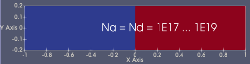
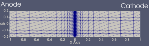
We use SemiVi ‘Structure generator and Mesher’ to create the diode structure and a finite-element mesh for the device. The structure is shown in Fig. 1(a).
(a)
Device
Structure |
(b)
Mesh |
The pn-diode structure consists of a Silicon stripe of 400nm width and 2μm length. The Si stripe is uniformly doped with n-doping of 1017cm-3 – 1019cm-3. A uniform mesh spacing of 100nm along y-direction. Due to the high field at the pn-junction, the junction is refined with the mesh spacing of 1Å along x-direction. Mesh gradually becomes coarse away from the junction. Mesh is shown in Fig. 1(b).
Both Anode and Cathode are assumed to be Ohmic contacts. All the simulations are performed by quasistationary ramp to -1V and then another quasistationary ramp to 1V. SemiVi drift-diffusion simulator is used for all the device simulations.
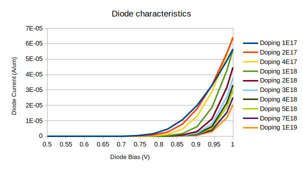
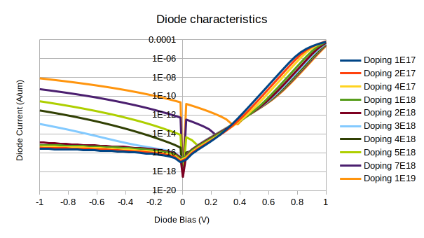
Current-voltage characteristics of the diode are shown in Fig. 2. On linear y-scale (see Fig. 2(a)), the diode characteristics look as expected. The diode forward voltage increases with the doping concentration, as expected from the theory of pn-diodes. Note, the exponential nature of the current arising from Thermionic emission mechanism at the pn-junction. This is a characteristic of a pn-diode.
I-V characteristics in the reverse bias of the diode (on log-scale, see Fig. 2(b)) show a higher reverse current when the doping is higher than 1018cm-3. This reverse current increases exponentially with the doping concentration. Above the doping of 1018cm-3, electric field at the pn-junction is higher than the critical field required for the onset of BTBT. As a result, above this doping, e-h generation by BTBT process begins. BTBT generation show exponential field dependence (see Eq. 1). Hence, as the doping increases, BTBT generation increases exponentially. At the doping of 1019cm-3, reverse current of the diode is as high as the forward current, owing to BTBT generation process.
(a)
Linear
y-axis |
(b)
Log
y-axis |
(a)
Magnitude
of
Electric
field |
(b)
BTBT
Generation
rate |
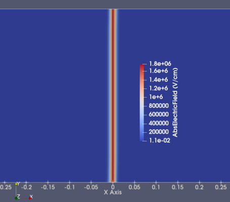
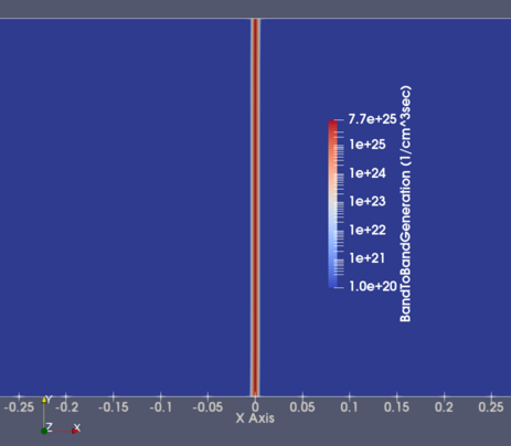
Spatial distribution of electric field in the pn-diode with doping of 1019cm-3 is plotted in Fig. 4(a) at the reverse bias of 1V. High field is present in the narrow region at pn-junction. It gives rise to BTBT generation at the junction. Spatial distribution of BTBT generation rate is shown in Fig. 4(b). It is distributed in the narrow area of high electric field.
(a)
Magnitude
of
Electric
field |
(b)
SRH
recombination
rate |
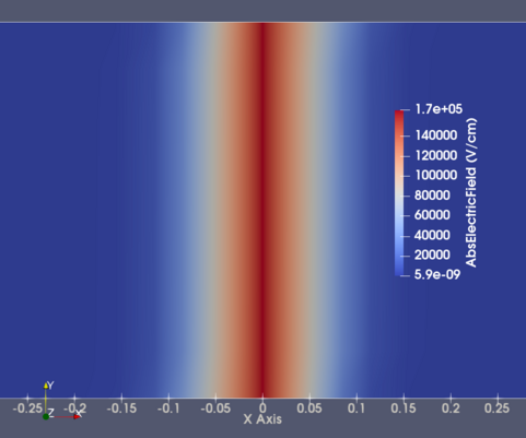
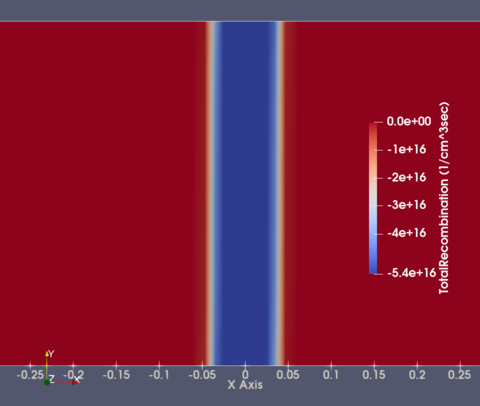
In comparison, spatial distribution of the field in the diode with doping of 1017cm-3 is plotted in Fig. 4(a). It is spread in the relatively wider region at the pn-junction. As the field does not cross threshold for BTBT generation, the BTBT rate is negligible in this device. Instead, the diode reverse current is caused primarily by e-h generation by SRH process as shown in Fig. 4(b).
A. Negative Differential Resistance
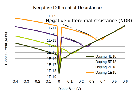
Simulated diode characteristics on log scale reveal a unique feature of the tunnel diodes - negative differential resistance (NDR). In
the diode with the doping of 1019 cm-3, current decreases from 10-11 A/μm to 10-13 A/μm as bias voltage increases from 0 to
400mV (see Fig. 5). In this region, differential resistance (i.e.  ) is negative, hence the name. This characteristics is used in analog
applications. Gunn diode is one such example of the application of NDR region.
) is negative, hence the name. This characteristics is used in analog
applications. Gunn diode is one such example of the application of NDR region.