Small-signal Analysis of a Double-gate MOSFET
Saurabh Sant
SemiVi LLC
Zurich, Switzerland.
saurabh.sant@semivi.ch
Abstract
A Silicon double-gate n-channel MOSFET is simulated using SemiVi drift-diffusion solver to obtain output- and transfer-
characteristics of the MOSFET. Mobility degradation due to interface roughness, doping, and high-field mobility saturation is
taken into account in the simulations. Additionally, AC analysis is performed on the MOSFET to extract various small-signal
parameters.
Index Terms
Double-gate MOSFET, drift-diffusion, n-channel, FinFET.
I. Introduction
Over the past years, Semiconductor VLSI industry has been transformed by ever-increasing density of MOSFETs packed on a
single chip. This was made possible by the scaling down of the MOSFET channel length. At smaller channel lengths,
a traditional planar MOSFET is no longer suitable, due to high leakage current. This is, in part, due to insufficient
electrostatic control of the channel by the single gate. Electrostatic control can be improved introducing two parallel gates on
opposite sides of the thin Silicon layer. Such a structure is difficult to realize in planar MOSFET design. Hence, a
FinFET is introduced, in which the gates are introduced on two sides of the vertical ‘fin-like’ structure - hence the
name.
In this work, we perform simulation study of a double-gate MOSFET (DG-MOSFET) to obtain both output- and transfer-
characteristics. Also, to extract small-signal parameters, we perform AC analysis of the MOSFET in the on-state.
II. Mobility Degradation in nano-scale MOSFET
As the source and the drain regions are heavily doped, resistance of a MOSFET often depends on the channel resistance. Presence of
impurities in the channel region increases scattering resulting in channel mobility degradation. In the SemiVi simulator, this is modeled
by activating Masetti model throughout the device.
Silicon/Gate-oxide interface often exhibits roughness, which adds to scattering of carriers in the inversion layer. This degrades
mobility of the carriers in the channel. This, surface-roughness induced mobility degradation is modeled by a model proposed by
Lombardi el al.
Carrier velocity is given by  = μ⋅
= μ⋅ , where
  is electric field.
  increases with
  . But this increase is sub-linear, and saturates at
high fields. This is due to the increased scattering at high electric field. This phenomenon is modeled by mobility saturation at “high
field”. We use a “High field saturation” model proposed by Canali el al.
. But this increase is sub-linear, and saturates at
high fields. This is due to the increased scattering at high electric field. This phenomenon is modeled by mobility saturation at “high
field”. We use a “High field saturation” model proposed by Canali el al.
The above models are implemented in ‘SemiVi’ drift-diffusion simulator and are activated throughout the device during the
simulations.
III. Simulation Setup
We use SemiVi ‘Structure generator and Mesher’ [2] to create the DG-MOSFET structure and mesh it using the built-in
mesher.
A. Device Structure
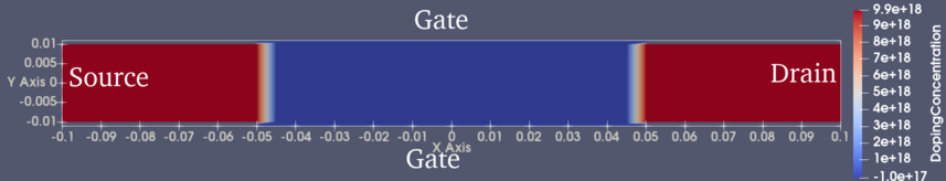
The DG-MOSFET consists of a Silicon layer of thickness 20 nm and channel length of 100 nm. Source and drain of the device have
50nm length. Silicon layer is doped with Boron doping of 1 × 10¹⁷/cm3, while source/drain are doped with Phosphorus doping of
1019/cm3. Gate-oxide is composed of SiO2 with the thickness of 2nm on top and bottom of the stripe. Device structure and the doping
concentration is shown in Fig. 1(b).
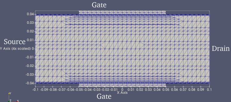
The device is meshed using ‘SemiVi’ mesher, which uses Quad-tree based ‘FEM meshing’. Since the channel region show sharp
changes in electron density, mesh near gate-oxide/Si interface is refined. Final mesh is shown in Fig. 1(a).
Transfer characteristics of the MOSFET are simulated by quasistationarily ramping the gate voltage from 0V to 1V at a constant
drain voltage. Similarly, output characteristics are simulated by quasistationarily ramping the drain voltage from 0V to 1V at a constant
gate voltage. SemiVi drift-diffusion simulator [3] is used for all the device simulations.
IV. Results and Discussion
A. Reverse bias characteristics
Transfer characteristics of the DG-MOSFET are plotted in Fig. 2 at different source-drain bias values (Vds). Linear scale
transfer plot (in Fig. 2(a)) shows threshold voltage (Vth) of approx. 0.5V. Semilog-Y plot of the transfer curves (in
Fig. 2(b)) shows constant slope in the sub-threshold region. This is a characteristic of thermionic emission - principle of
MOSFET switching. At room temperature, the sub-threshold swing is 60mV/decade. That is, per 60mV increase of
Vgs, drain current increases by an order of magnitude. When V ds < V gs - V th, MOSFET operates in linear regime
i.e. drain current depends on both Vgs and Vds. When V ds > V gs - V th, MOSFET operates in saturation region
- drain current is independent of Vds, and is proportional to (V gs - V th)2. The quantity V gs - V th is also called
‘over-voltage’.
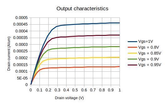
Output characteristics of the DG-MOSFET at fixed Vgs are plotted in Fig. 3 at different values of Vgs. The region where drain
current increase linearly with drain voltage is called linear region. When V ds > V gs - V th, the MOSFET enters saturation region
where drain current saturates. Even in the saturation region, a small slope is visible in the Id-Vd curve. This is due to ‘short-channel
effect’.
In this way, our simulations reveal various regions of the MOSFET characteristics.
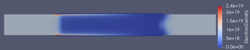
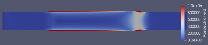
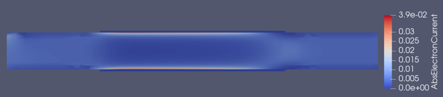
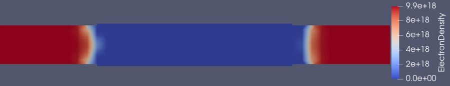
Spatial distribution of the magnitude of electric field | | throughout the device in the on-state (Vgs = 1V and Vds = 1V) is given in
Fig. 4(b). Maximum field appears in the oxide region. Spatial distribution of electron density is plotted in Fig. 4(a). Electron density is
highest in the channel regions - higher than source and drain! Along the channel, inversion electron density is high at the ‘source-end’
compared to the ‘drain-end’ of the channel. Absolute electron current in Fig. 4(c) shows high current density in the channel compared
to the bulk of the Silicon device.
| throughout the device in the on-state (Vgs = 1V and Vds = 1V) is given in
Fig. 4(b). Maximum field appears in the oxide region. Spatial distribution of electron density is plotted in Fig. 4(a). Electron density is
highest in the channel regions - higher than source and drain! Along the channel, inversion electron density is high at the ‘source-end’
compared to the ‘drain-end’ of the channel. Absolute electron current in Fig. 4(c) shows high current density in the channel compared
to the bulk of the Silicon device.
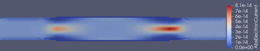
Spatial distribution of electron density and electron current density in the off-state (Vgs = 50mV and Vds = 1V) are shown in
Fig. 5(a) and Fig 5(b), respectively. No channel is formed, hence the channel region has negligible electron density. In the off-state,
current originates primarily from SRH recombination taking place at the p-n junctions. Also, current density is negligible, and
concentrated in the bulk of the device.
B. Small-signal characteristics
Small-signal parameters of the DG-MOSFET are extracted in the on-state of the DG-MOSFET by performing AC-analysis at
Vgs=1V and Vds=1V using the drift-diffusion simulator.
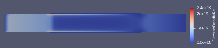
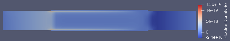
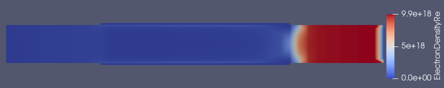
Spatial distribution of real part of small-signal variations in electron density arising from small-signal voltages (f = 1kHz) at
the source, gate, and drain are shown in Fig. 6. Comparing the effect of AC voltage at the source (Fig. 6(a)) and at
the drain (Fig. 6(c)) shows, that small variations in ∂V ds are confined to the drain. Due to the channel pinch off
at the channel-drain junction, the drain ‘electron well’ is secluded from the rest of the device resulting in such an
effect.
References
[1] R. van Overstraeten, H. de Man,“Measurement of the Ionization Rates in Diffused Silicon p-n Junctions,” Solid-State Electronics, vol. 13, no. 1, pp.
583–608, 1970.
[2] Structure Generator and Mesher User Guide, SemiVi LLC, Switzerland, 2025.
[3] Drift-diffusion Solver User Guide, SemiVi LLC, Switzerland, 2025.