 mbox . Channel region of the MOSFET is intrinsically n-doped with doping of
2 × 1016cm-3, whereas raised- source and drain regions are heavily n-doped. The gate-oxide is a high-k oxide with an equivalent oxide
thickness (EOT) of 8.5Å.
mbox . Channel region of the MOSFET is intrinsically n-doped with doping of
2 × 1016cm-3, whereas raised- source and drain regions are heavily n-doped. The gate-oxide is a high-k oxide with an equivalent oxide
thickness (EOT) of 8.5Å.
Floating body effect induced off-state leakage and on-state mobility degradation in scaled InGaAs planar MOSFETs
Saurabh Sant SemiVi LLC Zurich, Switzerland. saurabh.sant@semivi.ch
Abstract In0.53Ga0.47As -on-insulator MOSFETs exhibit floating body effect resulting in high off-state leakage. Floating body effect turns the parasitic BJT on, which weakly conducts current in the off-state of the MOSFET. Here, we perform drift-diffusion simulations of In0.53Ga0.47As -on-insulator planar and nanowire MOSFETs to understand this leakage mechanism. We show that band-to-band tunneling at the channel-drain junction supplies “base current” to the BJT, thereby turning it on.
Additionally, measured transfer characteristics show on-state current degradation of the MOSFETs at high gate bias. This is caused by channel mobility degradation in the MOSFETs. In this work, we model mobility degradation using “Lombardi model”. We calibrate the model to the measured transfer characteristics and provide a parameter set suitable for modeling mobility degradation in In0.53Ga0.47As channel devices.
Index Terms In0.53Ga0.47As planar MOSFETs, floating body effect, band-to-band tunneling, mobility degradation.
High electron mobility in In0.53Ga0.47As makes it a suitable material to replace Silicon channel in high performance MOSFETs. InGaAs-on-insulator MOSFETs are preferred over bulk InGaAs devices due to superior electrostatics as well as low gate capacitance. However, due to the absence of body bias, these MOSFETs suffer from floating body effect. This floating body effect gives rise to band-to-band tunneling (BTBT)turns on parasitic bipolar junction transistor (BJT) in the MOSFETs giving rise to high off-state leakage. Similarly, presence of gate-oxide (GOX) / InGaAs interface traps results in degradation of the gate-control of the channel.
Measurement of the on-state performance of fabricated planar In0.53Ga0.47As -OI MOSFETs reveals mobility of 300cm2/Vs in contrast with the literature value of 2000cm2/Vs in bulk In0.53Ga0.47As . Mobility degradation in In0.53Ga0.47As channel due to surface roughness and defects is responsible for low value of the measured mobility.
In this work, we use SemiVi drift-diffusion solver to simulate planar In0.53Ga0.47As -on-insulator MOSFETs. We compare the simulated transfer characteristics with the measured data of these devices to establish efficacy of the simulation results. We dis-entangle the observed transfer characteristics to highlight the effect of the above mentioned non-idealities. Also, we model channel mobility degradation by using “Lombardi model”.
The planar In0.53Ga0.47As -on-insulator MOSFETs simulated in this work were fabricated using a CMOS-compatible self-aligned
replacement-metal-gate process. The fabrication process is described in [3] and [4]. The process is designed to fabricate
ultra-thin-body MOSFETs with variable widths. Here, we have selected the MOSFETs with 500nm width for the simulation. Since the
MOSFET structure is invariant along the width, 2D cross-section of the MOSFET with LG = 13nm, 100nm, and 300nm are generated
and meshed by using SemiVi structure generator and mesher [5]. The device structure and the doping profiles of LG = 13nm
MOSFET are shown in Fig. mbox II-Ambox . Channel region of the MOSFET is intrinsically n-doped with doping of
2 × 1016cm-3, whereas raised- source and drain regions are heavily n-doped. The gate-oxide is a high-k oxide with an equivalent oxide
thickness (EOT) of 8.5Å.
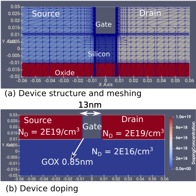 Fig. 1. (a) Structure and mesh of the simulated device with LG = 13nm. Similar devices with LG = 130nm, 300nm are simulated. (b) Dopant distribution
in the simulated device with LG = 13nm.
Fig. 1. (a) Structure and mesh of the simulated device with LG = 13nm. Similar devices with LG = 130nm, 300nm are simulated. (b) Dopant distribution
in the simulated device with LG = 13nm.
Interface defects present at the high-k GOX/In0.53Ga0.47As as well as interface roughness degrade channel mobility considerably below its bulk value. In this work, hole mobility in the channel is set to a fixed value of 80 cm2/Vs. Following literature, bulk electron mobility is set to 2000cm2/Vs. Channel mobility degradation is modeled using “Lombardi model”.
The biasing conditions give rise to a high electric filed at the channel-drain junction generating electron and hole pairs due to high BTBT. This is modeled by the nonlocal BTB tunneling model available in the drift-diffusion solver. This model uses Wentzel-Kramer-Brillouin (WKB) approximation to calculate transmission probability and tunnel rates along the nonlocal paths. Electron and hole tunnel masses are set to 0.043 m0 and 0.052 m0. Electron and hole lifetimes in the material are set to 1 ns.
Donor-type interface defects are simulated at the GOX/In0.53Ga0.47As interface with a uniform distribution in the band gap. Defect density (Dit) is set to 2 × 10¹²/cm2eV which fits the measured subthreshold swing of log-channel MOSFETs at VDS = 50mV.
Quantum confinement moves electron density away from the GOX/InGaAs interface. This effect is modeled in the drift-diffusion simulations using modified local density approximation (MLDA).
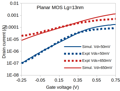
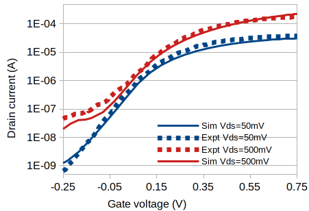
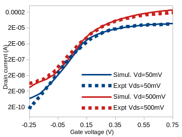
Comparison of the simulated transfer characteristics of the planar MOSFETs with the measurements is shown in Figs. 2(a), 2(b), and 2(c), for LG = 13nm, 100nm, and 300nm, respectively. The figures show good match between measured and simulated transfer characteristics.
(a)
LG =
13nm |
(b)
LG =
100nm |
(c)
LG =
300nm |
A. Effect of band-to-band tunneling
Due to high electric field, BTBT takes place at the channel-drain interface generating electron and hole pairs. This mechanism supplies hole current to the base of the n-p-n parasitic BJT under the MOSFET, with channel as base. This turns on the BJT and causes off-state leakage. The injected holes recombine at the source-channel junction which is nothing but the emitter/base junction. Spatial distribution of BTBT electron and hole generation rate and SRH recombination rate, shown in Fig. 3 reveals this phenomenon.
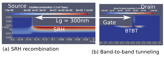 Fig. 3. Spatial distribution of (a) SRH recombination rate, and (b) BTB tunneling rate is plotted at the source-channel and at the drain-channel junction,
respectively. The plots are made in the off-state (Vg = -0.25V and Vd = 0.65V. LG = 300nm. A schematic of parasitic BJT is also shown. BTB tunneling
at the channel-drain junction acts as a source of hole current to the base of the BJT and turns it on, which leads to higher leakage currents. Source-channel
junction coincides with the base-emitter junction of the BJT, thus exhibiting high SRH recombination rate.
Fig. 3. Spatial distribution of (a) SRH recombination rate, and (b) BTB tunneling rate is plotted at the source-channel and at the drain-channel junction,
respectively. The plots are made in the off-state (Vg = -0.25V and Vd = 0.65V. LG = 300nm. A schematic of parasitic BJT is also shown. BTB tunneling
at the channel-drain junction acts as a source of hole current to the base of the BJT and turns it on, which leads to higher leakage currents. Source-channel
junction coincides with the base-emitter junction of the BJT, thus exhibiting high SRH recombination rate.
B. Effect of interface defects
Interface traps at GOX/In0.53Ga0.47As interface reduce electrostatic coupling between the gate and the channel, resulting in higher subthreshold swing. Interface trap density (Dit) at the GOX/InGaAs interface is set by fitting the simulations to the subthreshold region of the transfer characteristics. A uniform Dit = 2 × 1012cm-2eV-1 in the channel gives best fit to the measured data at VDS = 50mV. Such a high Dit increases electric field at the channel-drain interface causing higher leakage. This is seen in the transfer characteristics of the plane MOSFETs with LG =300nm simulated with and without interface defects (See Fig. 4)
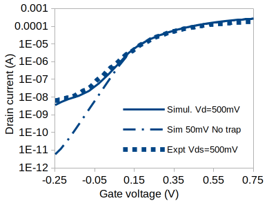 Fig. 4. Effect of GOX-In0.53Ga0.47As interface traps is shown by plotting the transfer characteristics with and without the traps (LG = 300nm).
C. Channel mobility degradation due to normal field
Measured electron mobility in In0.53Ga0.47As MOSFETs is 300cm2/Vs, whereas reported bulk mobility in In0.53Ga0.47As is 2000cm2/Vs, at a high doping of 5 × 1018cm-3. This reflects severe mobility degradation in the channel of the MOSFETs. This degradation is caused by electron scattering due to surface roughness and interface defects. In this work, channel mobility degradation is modeled by Lombardi model [7]. The model parameters are fitted to match the experimental transfer characteristics at VDS = 50mV of the planar MOSFET of gate length 300nm. Transfer characteristics of the long channel planar MOSFET obtained using these parameters are plotted in Fig 5 and are compared with the measured data.
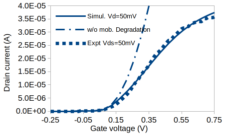 Fig. 5. Simulated and measured transfer characteristics of the planar In0.53Ga0.47As -on-insulator MOSFET (LG =300nm and W = 500nm) using Lombardi
model for channel mobility degradation. Dash-dotted lines show the transfer characteristics simulated by deactivating Lombardi model.
Fig. 5. Simulated and measured transfer characteristics of the planar In0.53Ga0.47As -on-insulator MOSFET (LG =300nm and W = 500nm) using Lombardi
model for channel mobility degradation. Dash-dotted lines show the transfer characteristics simulated by deactivating Lombardi model.
[1] M. Yoshimi et al.,“Suppression of the floating-body effect in SOI MOSFET’s by the bandgap engineering method using a Si1-xGex source structure” IEEE Trans. Electron Devices, vol. 44, no. 3, pp. 423–430, Mar. 1997.
[2] J. Lin, D. A. Antoniadis, and J. A. del Alamo,“Off-state leakage induced by band-to-band tunneling and floating-body bipolar effect in InGaAs quantum-well MOSFETs,” IEEE Electron Device Lett., vol. 35, no. 12, pp. 1203–1205, Dec. 2014.
[3] H. Hahn et al., “A scaled replacement metal gate InGaAs-on-Insulator n-FinFET on Si with record performance,” in Proc. IEEE IEDM, Dec. 2017, pp. 17.5.1–17.5.4.
[4] V. Deshpande et al., “First demonstration of 3D SRAM through 3D monolithic integration of InGaAs n-FinFETs on FDSOI Si CMOS with inter-layer contacts,” in Proc. IEEE Symp. VLSI Technol., Jun. 2017, pp. T74–T75.
[5] Structure Generator and Mesher User Guide, SemiVi LLC, Switzerland, 2025.
[6] Drift-diffusion Solver User Guide, SemiVi LLC, Switzerland, 2025.
[7] C. Lombardi et al., “A Physically Based Mobility Model for Numerical Simulation of Non-planar Devices,” IEEE Trans. Computer-Aided Design, vol. 7, no. 11, pp. 1164-1171, 1988.