(a)
Traditional
photo-diode |
(b)
Traditional
photo-diode
with
two
Silver
stripes
on its
top |
(c)
Close-up
image
of the
two
Silver
stripes |
Simulation of Plasmonic Photodiode Using FDTD simulations
Saurabh Sant SemiVi LLC Zurich, Switzerland. saurabh.sant@semivi.ch
Abstract We present study of Silicon waveguide which terminates at a InGaAs photo-diode with and without plasmonic enhancement. In this study, FDTD simulations are performed together with solving Drude equation in the metallic stripes. The study shows that adding metallic stripes on the top of InGaAs photo-diode changes the field distribution in the photodiode. The waveguide mode couples with the plasmonic mode exhibited by the metallic stripes. This results in field enhancement near the stripes.
Index Terms Silicon photonics, photodiode, plasmonic mode, hardware-accelerated FDTD solver.
Recent advancements in AI have brought the necessity of large data-centers to the forefront. High-speed optical data-receivers in these datacenters requires ultra-fast and broad-band detection of optical signals. Monolithically integrated photodiodes (PD) are well suited for the receiver applications. Performance and speed of the PDs can be improved by shrinking the structure. Structure shrinkage while still ensuring sufficient coupling strength can be achieved by utilizing a photo-diode with plasmonic enhancement. In this study, we design a butt-coupled waveguide photodetector and study the impact of enhancing the photodiode with the plasmonic mode between two Silver stripes on the top of it. For the structure design and simulation, we use the hardware-accelerated FDTD simulator by SemiVi.
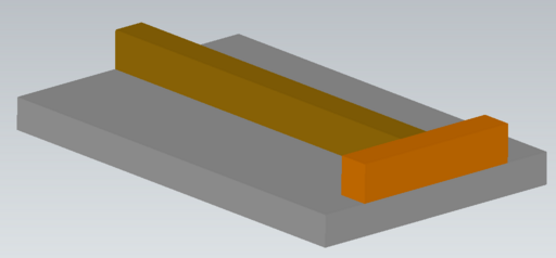
In order to study the effect of plasmonic structures on coupling strength of the photodiode, we performed a comparative study of two photo-diode geometries - traditional InGaAs photodiode structure, and the InGaAs structure + two Silver stripes on the top of it. The two structures are shown in Fig. 1. Note that, the waveguide and the diode are located on the top of an oxide slab. The simulation domain is defined by a cubic box of ‘vacuum’ around the structure such that there is padding of 0.22μm on all sides of the cuboid.
|
(a)
Traditional
photo-diode |
|
(b)
Traditional
photo-diode
with
two
Silver
stripes
on its
top |
|
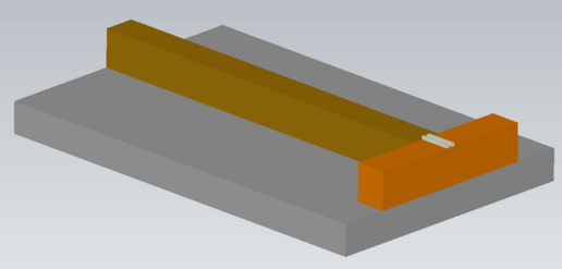
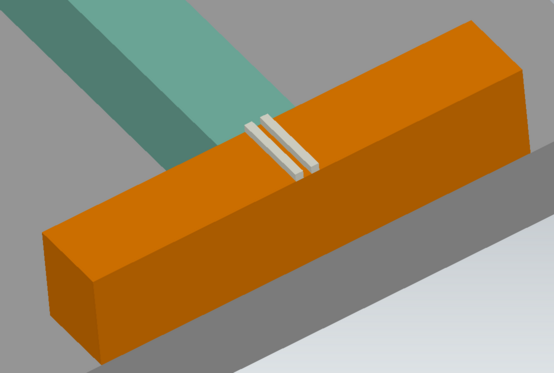
(c)
Close-up
image
of the
two
Silver
stripes |
The waveguide cross-section of 200nm x 240nm is used for this study. The rectangular structure has a side-length of 1.1μm in the transverse direction and a cross-section of 200nm x 240nm. In both the structures, the waveguide touches the photodiode at the termination point. Cubic grid-spacing of 20nm is used along x,y,z axes in all the FDTD simulations.
In plasmonic structure, two Silver stripes of cross-section 20nm x 20nm are placed on the top of the photodiode in the direction of the waveguide (x-direction). Spacing between the two stripes is 20nm. This creates a plasmonic mode between the two stripes. The waveguide mode couples with the plasmonic mode once it enters the photodiode. In the region of the Silver stripes, mesh spacing in y- and z- directions is decreased to 2.5nm to ensure that the plasmonic mode is modeled.
B. Light source and boundary conditions
Coupling strength of waveguide and photo-diode structures is probed by exciting the waveguide by a uniform plane-wave source at 200nm away from the end. The source of intensity 1000W and wavelength of 1.35μm, was placed in the plane perpendicular to the waveguide and was confined to the cross-section of the waveguide.
Convolutional perfectly matched layer (CPML) boundary conditions (BCs) were active at all the boundaries of the simulation domain. The CPML BCs were active on the last ten boundary layers. All the boundary layers were located in the ‘vacuum’ padding.
Dielectric response in metals such as Silver is determined by Drude equation. In the FDTD solver, Drude equation is solved by using Auxiliary Differential Equation (ADE) method. In this method, frequency domain Drude equation is converted to time-domain equation as follows.
| χ(ω) | =  | (1) |
 (ω) (ω) | = ϵ0χ(ω) ⋅ (ω) (ω) | (2) |
 = jω = jω (ω) (ω) | =   (ω) (ω) | (3) |
Substituting jω → ,
,
 | (4) |
The above equation is solved at each grid-point to determine time evolution of electric field in dispersive media such as Silver stripes.
The above structures and mesh are created by the Python interface of the ‘Structure Generator and Mesher’ by SemiVi. It is simulated using the hardware-accelerated FDTD simulator by SemiVi. Nvidia GPU ‘GTX3090’ is used for FDTD simulations. The simulator stores the results in hdf format and write a xdmf script file which can be opened in ‘Paraview’.
FDTD simulations are performed for 200 fsec. At time of 180 fsec, spatial intensity is calculated in the photo-diode. Also, between time 180 fsec to 200 fsec, spatial electric field is time-averaged only in the photo-diode structure. Spatial distribution of time-averaged electric field in the YZ-section (perpendicular to the direction of Silver stripes) in the photo-diode is shown in Fig. 2.
Note, that electric field is concentrated around the bottom of Silver stripes in the structure with the stripes. Whereas, in the traditional photo-diode structure, electric field is uniformly distributed in the photo-diode. Two parallel silver stripes give rise to a plasmonic mode in between them. Waveguide mode is coupled to this plasmonic mode giving rise to such a peculiar distribution of electric field around Silver stripes.
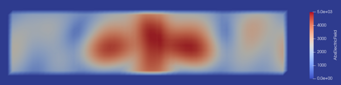
(a)
Without
Silver
stripes |

(b)
With
Silver
stripes |