
Simulation of forward characteristics and reverse breakdown characteristics of Silicon power diodes
Saurabh Sant SemiVi LLC Zurich, Switzerland. saurabh.sant@semivi.ch
Abstract A Silicon power diode with non-punchthrough P-i-N design is simulated using SemiVi drift-diffusion solver under both forward and reverse bias conditions. The power diode is intrinsically Boron doped with doping of 1016cm-3. To simulate reverse breakdown characteristics of the diode, van Overstraeten model is activated and its parameters are set to their default values. The diode yields breakdown voltage of 62V for Boron intrinsic doping of 1016cm-3. The intrinsic doping is varied from 1E15 to 1E17 to analyze breakdown voltage variation with intrinsic doping.
Index Terms Power diode, drift-diffusion, non-punchthrough design, PiN diode.
Power diode is typically used in an asynchronous rectifier circuit, in reverse bias with the Insulated Gate Bipolar Transistor (IGBT), and in various other power electronic applications. It is also called PiN diode, because it consists of p-doped region followed by thick intrinsic Silicon, which is followed by n-doped region. Due to the thick intrinsic region, the diode can block large reverse voltage. Despite the presence of thick intrinsic region, PiN Power diode offers ultra-low resistance in forward bias owing to plasma accumulation in the intrinsic region.
In forward biased p-i-n diode, current is conducted by both electrons and holes in the intrinsic region, called bipolar transport. When the diode changes polarity, e-h plasma in the intrinsic region must be removed. This removal of e-h plasma is slow, which results in lower operating frequecy of the PiN diode.
In this work, we perform drift-diffusion simulations of a PiN diode. We analyze both forward and reverse bias characteristics of the diode. Also, we determine breakdown voltage of the diode. For that purpose, we use van Overstraeten model for modeling breakdown regime.
II. Modeling Avalanche Breakdown
In the presence of extremely high electric field, electrons are sufficiently accelerated to eject more electrons from the Valence Band (VB) to the Conduction Band (CB), thereby creating an electron-hole pair in the semiconductor. The generated electrons also undergo acceleration and subsequent collision with electrons in VB generating more e-h pairs. Similar process takes place for holes.
Generation rate for the impact ionization process can be expressed as follows.
|
| (1) |
Here,  and
and  are magnitudes of e and h current densities while αn and αp are ionization coefficients of e and h,
respectively.
are magnitudes of e and h current densities while αn and αp are ionization coefficients of e and h,
respectively.
The ionization coefficients αn and αp strongly depend on the electric field parallel to the carrier transport direction. In the model presented by Van Overstraeten et. al. [1], it is modeled by the following expression.
 | (2) |
Here, an∕p and bn∕p in Eq. 2 are the model parameters, and Fava is magnitude of the electric field parallel to the carrier transport direction.
The above model is used to calculate e-h generation rate in ‘SemiVi’ drift-diffusion simulator.
We use SemiVi ‘Structure generator and Mesher’ [2] to create the P-i-N diode structure and mesh it using the built-in mesher.
 Fig. 1. Structure of the P-i-N diode simulated in this paper. Note, for ease of visualization, the structure is scaled by a factor of 10 along X-axis. Doping
of the intrinsic region is varied to get different breakdown voltage.
Fig. 1. Structure of the P-i-N diode simulated in this paper. Note, for ease of visualization, the structure is scaled by a factor of 10 along X-axis. Doping
of the intrinsic region is varied to get different breakdown voltage.
The p-i-n diode structure consists of a Silicon stripe of 2μm width and 20μm length. The Si stripe is uniformly doped with p-doping of 1016cm-3. A uniform mesh spacing of 100nm along x-direction, and a spacing of 25nm along y-direction, which is also a transport direction.
Reverse bias characteristics are simulated by a quasistationary ramp from 0V to -100V. Forward bias characterisics are simulated separately by a quasistationary ramp from 0V to 5V. SemiVi drift-diffusion simulator [3] is used for all the device simulations.
A. Reverse bias characteristics
Current-voltage characteristics of the p-i-n diode in reverse bias are shown in Fig. 2. On log y-scale (see Fig. 2(b)), the diode characteristics look as expected with the diode breakdown voltage of 62V. At both 62V and 70V reverse bias, a kink is visible in the I-V characteristics. This is due to the onset of breakdown at n-i junction near Cathode. Note, that although only electron current at the Cathode is plotted here, an equal amount of hole current flows to the Anode.
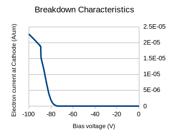
(a)
Electron
current
(linear
y-axis) |
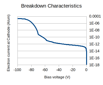
(b)
Electron
current
(log
y-axis) |
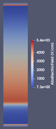
Spatial distribution of the magnitude of electric field | | throughout the device is given in Fig. 3(c) and Fig. 3(d). Maximum field
appears at the n-i junction close to Cathode. The figures show that maximum electric field at -30V bias is lower than critical electric
field, whereas maximum field in the device at -61V is higher than critical field. Subsequntly, avalanche generation also
appears at the n-i junction close to Cathode. A close look at the scales of avalanche generation rate at -30V and at
-61V reveal that, at the latter bias point, avalanche generation at -61V is an order of magnitude higher than that at
-30V.
| throughout the device is given in Fig. 3(c) and Fig. 3(d). Maximum field
appears at the n-i junction close to Cathode. The figures show that maximum electric field at -30V bias is lower than critical electric
field, whereas maximum field in the device at -61V is higher than critical field. Subsequntly, avalanche generation also
appears at the n-i junction close to Cathode. A close look at the scales of avalanche generation rate at -30V and at
-61V reveal that, at the latter bias point, avalanche generation at -61V is an order of magnitude higher than that at
-30V.
(a)
Impact
ionization
at
-30V |
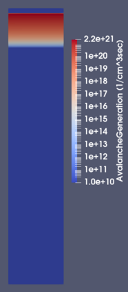
(b)
Impact
ionization
at
-61V |
(c)
Abs.
electric
field at
-30V |
(d)
Abs.
electric
field at
-61V |
Spatial distribution of electron and hole current densities is shown in Fig. 4(a) and Fig 4(b), respectively. Since the device is already in avalanche generation mode, both electron and hole currents appear to originate at the n-i junction. A large number of e-h pairs are generated at n-i junction and drift away towards cathode and anode.
(a)
Electron
current
at
-61V |
|
(b)
Hole
current
at
-61V |
B. Forward bias characteristics
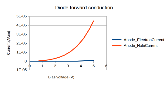
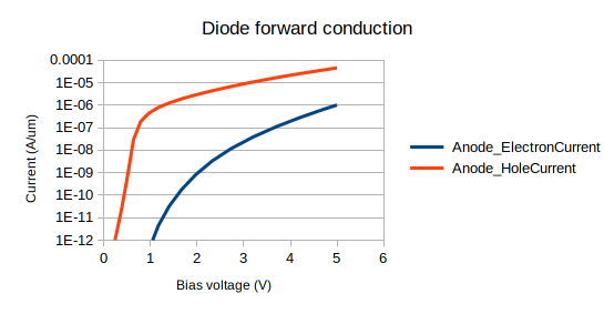
Forward bias I-V characteristics of the p-i-n diode are plotted in Fig. 5(a) and Fig. 5(b), on linear y-scale and log scale, respectively. Both, electron current and hole current at the anode are plotted versus forward bias. The figure confirms built-in voltage of the diode is approx 0.7V. In forward bias, anode current consists mainly of holes, whereas cathode current consists mainly of electrons. This is visible in the I-V plots.
(a)
Current
on
linear
y-axis |
(b)
Current
on log
y-axis |
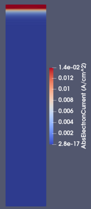
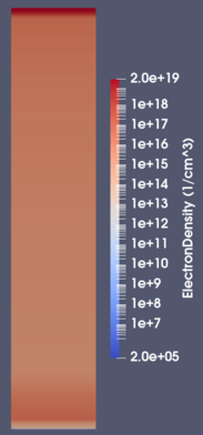
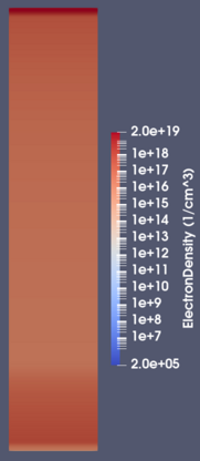
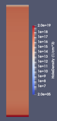
Spatial distribution of electron and hole densities at forward bias of 2.5V and 5V are shown in Figs. 6. The figures show that electron and hole densities overlap in the intrinsic region. This suggests that e-h plasma has developed in the diode in the forward bias.
(a)
Electron
density
at
2.5V |
(b)
Electron
density
at 5V |
(c)
Hole
density
at
2.5V |
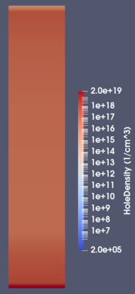
(d)
Hole
density
at 5V |
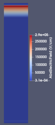
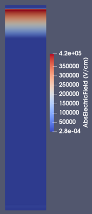
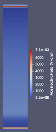
Spatial distribution of magnitude of electric field in the p-i-n diode is shown in Fig. 7(a) and Fig. 7(b) at a forward bias of 2.5V and 5V respectively. At a lower bias, maximum electric field is present at the n-i junction close to cathode. However, at high forward bias, due to high current flow, electric field is nearly ‘uniformly’ distributed throughout the intrinsic region.
(a)
Electric
field at
2.5V |
(b)
Electric
field at
5V |
[1] R. van Overstraeten, H. de Man,“Measurement of the Ionization Rates in Diffused Silicon p-n Junctions,” Solid-State Electronics, vol. 13, no. 1, pp. 583–608, 1970.
[2] Structure Generator and Mesher User Guide, SemiVi LLC, Switzerland, 2025.
[3] Drift-diffusion Solver User Guide, SemiVi LLC, Switzerland, 2025.