
Simulation of turn-on and turn-off transients of Silicon power diodes
Saurabh Sant SemiVi LLC Zurich, Switzerland. saurabh.sant@semivi.ch
Abstract Turn-off and turn-on transient of a Silicon power diode with non-punchthrough P-i-N design is simulated using SemiVi drift-diffusion solver. The power diode is a non-punch-through design, intrinsically Boron doped with doping of 1016cm-3. To simulate reverse breakdown characteristics of the diode, van Overstraeten model is activated and its parameters are set to their default values. The diode yields breakdown voltage of 62V for Boron intrinsic doping of 1016cm-3.
Index Terms Power diode, drift-diffusion, non-punchthrough design, PiN diode, turn-on transients, turn-off transients.
Power diode is typically used in an asynchronous rectifier circuit, in reverse bias with the Insulated Gate Bipolar Transistor (IGBT), and in various other power electronic applications. It is also called PiN diode, because it consists of p-doped region followed by thick intrinsic Silicon, which is followed by n-doped region. Due to the thick intrinsic region, the diode can block large reverse voltage. Despite the presence of thick intrinsic region, PiN Power diode offers ultra-low resistance in forward bias owing to plasma accumulation in the intrinsic region.
In forward biased p-i-n diode, current is conducted by both electrons and holes in the intrinsic region, called bipolar transport. When the diode changes polarity, e-h plasma in the intrinsic region must be removed. This removal of e-h plasma is slow, which results in lower operating frequency of the PiN diode.
In this work, we perform drift-diffusion simulations of a PiN diode. We analyze transient characteristics of the power diode. to model impact ionization and avalanche breakdown, we use van Overstraeten model for modeling breakdown regime.
II. Modeling Avalanche Breakdown
In the presence of extremely high electric field, electrons are sufficiently accelerated to eject more electrons from the Valence Band (VB) to the Conduction Band (CB), thereby creating an electron-hole pair in the semiconductor. The generated electrons also undergo acceleration and subsequent collision with electrons in VB generating more e-h pairs. Similar process takes place for holes.
Generation rate for the impact ionization process can be expressed as follows.
|
| (1) |
Here,  and
and  are magnitudes of e and h current densities while αn and αp are ionization coefficients of e and h,
respectively.
are magnitudes of e and h current densities while αn and αp are ionization coefficients of e and h,
respectively.
The ionization coefficients αn and αp strongly depend on the electric field parallel to the carrier transport direction. In the model presented by Van Overstraeten et. al. [1], it is modeled by the following expression.
 | (2) |
Here, an∕p and bn∕p in Eq. 2 are the model parameters, and Fava is magnitude of the electric field parallel to the carrier transport direction.
The above model is used to calculate e-h generation rate in ‘SemiVi’ drift-diffusion simulator.
We use SemiVi ‘Structure generator and Mesher’ [2] to create the P-i-N diode structure and mesh it using the built-in mesher.
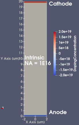 Fig. 1. Structure of the P-i-N diode simulated in this paper. Note, for ease of visualization, the structure is scaled by a factor of 10 along X-axis. Doping
of the intrinsic region is varied to get different breakdown voltage.
Fig. 1. Structure of the P-i-N diode simulated in this paper. Note, for ease of visualization, the structure is scaled by a factor of 10 along X-axis. Doping
of the intrinsic region is varied to get different breakdown voltage.
The p-i-n diode structure consists of a Silicon stripe of 2μm width and 20μm length (see Fig. 1). The Si stripe is uniformly doped with p-doping of 1016cm-3. A uniform mesh spacing of 100nm along x-direction, and a spacing of 25nm along y-direction, which is also a transport direction.
Transient turn-off of the diode is simulated as follows. First, quasistationary simulations are performed to forward bias the diode with the bias voltage of 2V. Then, anode is ramped from 2V down to -30V in 1 nano-seconds (ns). It is held at -30V for 1ns more, to study the effect of rapid turn-off on the off-state characteristics.
Transient turn-on of the diode is simulated by first performing quasistationary simulations to reverse bias the diode to -5V. Then, anode is ramped from -5V to 2V in 100ns. It is held at 2V for 100ns more.
SemiVi drift-diffusion simulator [3] is used for all the device simulations.
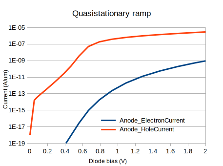
Forward I-V characteristics of the diode, which are simulated by the initial quasistationary ramp, are shown in Fig. 2(a). The I-V plots confirm diode forward voltage of 0.7V. In this ramp, e-h plasma is built up in the intrinsic region. This plasma needs to be swept away in order to turn-off the diode.
Transient electron and hole currents during turn-off of the p-i-n diode are shown in Fig. 2(b). As seen in the plot, electron and hole currents reach peak during the transient ramping down of the anode voltage. After that, diode current settles down to a small value, as expected in the reverse biased diode.
Peak in the turn-off transient current of the diode is due to the ‘emptying’ of the plasma. Due to the external field, electrons and holes, which were accumulated in the intrinsic region during the on-state, drift towards the cathode and the anode, respectively. They give rise to the transient current peaks at the respective electrodes, as shown in Fig. 2(b). Once e-h plasma is fully drained, the diode current comes down to a small value, arising from Shockley-Read-Hall (SRH) recombination and impact-ionization.
(a)
Quasistationary
ramp |
| (b)
Turn-off
Transients |
Spatial distribution of the magnitude of electric field |![]() | throughout the device is shown in Fig. 3(a), Fig. 3(b), and Fig. 3(c), at
0ns, 0.5ns, and 1ns, respectively. At the start of the ramp, the device is in forward bias, resulting in small field at p-i and i-n junctions.
As the diode turns off, electric field builds up at n-i junction near Cathode.
| throughout the device is shown in Fig. 3(a), Fig. 3(b), and Fig. 3(c), at
0ns, 0.5ns, and 1ns, respectively. At the start of the ramp, the device is in forward bias, resulting in small field at p-i and i-n junctions.
As the diode turns off, electric field builds up at n-i junction near Cathode.
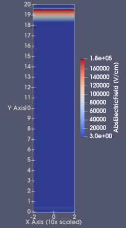
(a)
Abs.
electric
field at
time =
0ns |
|
(b)
Abs.
electric
field at
time =
0.5ns |
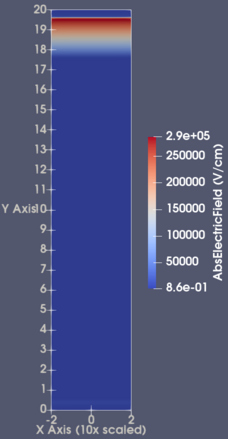
(c)
Abs.
electric
field at
time =
1ns |
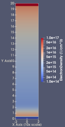
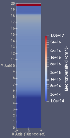
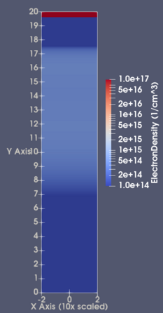
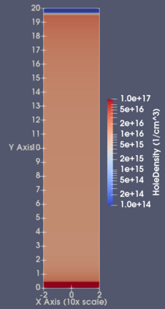
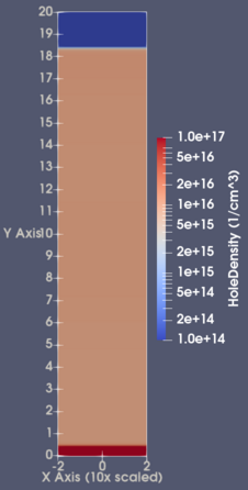
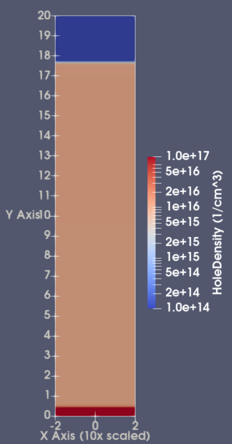
Time evolution of spatial distribution of electron and hole densities is shown in Fig. 4 and Fig. 5, respectively. At the start of the ramp, e-h plasma is seen built up in the intrinsic region. As the diode is more and more reverse biased, both electron and hole densities in the intrinsic region decline by two mechanisms - drift to the electrodes, and SRH recombination. However, this decline is not instantaneous! It is limited by finite mobilities, and finite recombination rates. As a result, a fraction electron density is still present in the intrinsic region, as shown in Fig. 4(c).
(a) t =
0 ns |
(b) t =
0.5 ns |
(c) t =
1 ns |
(a) t =
0 ns |
(b) t =
0.5 ns |
(c) t =
1 ns |
To study turn on transients, the diode is reverse biased to -5V at the beginning of the transient ramp. Then, anode voltage is ramped up to 2V in 100ns. Resulting transients are shown in Fig. 6.
[1] R. van Overstraeten, H. de Man,“Measurement of the Ionization Rates in Diffused Silicon p-n Junctions,” Solid-State Electronics, vol. 13, no. 1, pp. 583–608, 1970.
[2] Structure Generator and Mesher User Guide, SemiVi LLC, Switzerland, 2025.
[3] Drift-diffusion Solver User Guide, SemiVi LLC, Switzerland, 2025.