
Quantum Confinement in Si-channel Nanowire MOSFETs
Saurabh Sant SemiVi LLC Zurich, Switzerland. saurabh.sant@semivi.ch
Abstract Gate-all-around nanowire MOSFETs exhibit excellent gate control of the channel. However, quantum confinement in Silicon channel moves peak electron concentration away from oxide/Silicon interface. This reduces on-state current of the MOSFETs. Quantum effects are not readily taken into account in the drift-diffusion framework. Various models have been developed to include these effects in the framework. SemiVi drift-diffusion simulator models quantum confinement effects using Van-Dort, modified local density approximation, and density gradient models.
Index Terms Nanowire MOSFETs, Silicon, quantum confinement, mobility degradation.
Silicon channel FinFET scaling has reached its limit. Further scaling can be achieved by changing the device geometry from FinFET to a Gate-all-around (GAA) nanowire FET. In this work, one such GAA-FET is studied by TCAD simulations using SemiVi drift-diffusion solver. Quantum confinement in the channel moves peak electron (hole) concentration in n-FET (p-FET) away from oxide/Silicon interface. This degrades gate control of the channel and also reduces On-current. This work models quantum confinement using three different models available in the literature - Van Dort model, Modified Local Density Approximation (MLDA) model, and Density Gradient method.
II. Modeling quantum confinement
In this model, quantum potential is defined as follows.
|
| (1) |
where ϵr relative permittivity of the semiconductor, ϵ0 is permittivity of free space, kT thermal voltage, F⊥ is local electric field
normal to the nearest oxide/semiconductor interface. The parameters β and Fcrit are calibration parameters. f(| |) is a function of the
distance of the vertex from the interface, given by.
|) is a function of the
distance of the vertex from the interface, given by.
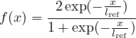 | (2) |
In this model, quantum potential is defined at each vertex in the region as follows.
 | (3) |
Here, d⊥ is the distance of the vertex from nearest insulator/semiconductor interface and λn∕p is thermal wavelength given by,
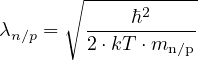 | (4) |
Here, mn∕p is the quantum confinement mass which is taken as a fitting parameter.
In this approach, quantum potential is defined by a function of the gradient of carrier density, hence the name density gradient. In this approach, quantum potential is defined as,
| Λn | = -  | (5) |
= - 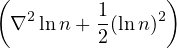 | (6) |
Here, mn∕p is the quantization effective mass, me is free electron mass, n is electron density. In second part of Eq. 5, the quantized effective mass is replaced by a fitting parameter γ.
Defining electron density with Boltzmann distribution (n = ni exp ), Eq. 5 can be reformulated as
follows.
), Eq. 5 can be reformulated as
follows.
 | (7) |
where u =  . Notice, that the solution term Λn exists on both sides of Eq. 7. Additionally, RHS of Eq. 7 depends on
logarithm of electron density n, whereas n depends on Λn. Hence, the above equation must be solved together with Poisson and carrier
continuity equation.
. Notice, that the solution term Λn exists on both sides of Eq. 7. Additionally, RHS of Eq. 7 depends on
logarithm of electron density n, whereas n depends on Λn. Hence, the above equation must be solved together with Poisson and carrier
continuity equation.
The Si nanowire MOSFETs simulated in this work were fabricated using a CMOS-compatible self-aligned replacement-metal-gate
process. The fabrication process is described in [?] and [?]. The process is designed to fabricate ultra-thin-body MOSFETs with
variable widths. Here, we have selected the MOSFETs with 500nm width for the simulation. Since the MOSFET structure is invariant
along the width, 2D cross-section of the MOSFET with LG = 13nm, 100nm, and 300nm are generated and meshed by using SemiVi
structure generator and mesher [1]. The device structure and the doping profiles of LG = 13nm MOSFET are shown in
Fig. mbox III-A mbox . Channel region of the MOSFET is intrinsically n-doped with doping of 2 × 1016cm-3, whereas raised-
source and drain regions are heavily n-doped. The gate-oxide is a high-k oxide with an equivalent oxide thickness (EOT) of
8.5Å.
mbox . Channel region of the MOSFET is intrinsically n-doped with doping of 2 × 1016cm-3, whereas raised-
source and drain regions are heavily n-doped. The gate-oxide is a high-k oxide with an equivalent oxide thickness (EOT) of
8.5Å.
The Si nanowire p- and n-MOSFETs are simulated in this work using cylindrical coordinate system. 2D radial cross-sections
of the devices with LG = 300nm are created using SemiVi structure generator and mesher [1]. These devices are
simulated using SemiVi drift-diffusion solver [2] with the Cylindrical coordinate system. The device structure and
the doping profiles of LG = 300nm n-MOSFET are shown in Fig. mbox III-A mbox . Channel-region of both p-
and n-MOSFET is n-doped with doping of 2 × 1016cm-3, whereas raised-source and drain regions are heavily n- or
p-doped in n- or p-MOSFETs, respectively. Gate-oxide is modeled as SiO2 with an equivalent oxide thickness (EOT) of
8.5Å.
mbox . Channel-region of both p-
and n-MOSFET is n-doped with doping of 2 × 1016cm-3, whereas raised-source and drain regions are heavily n- or
p-doped in n- or p-MOSFETs, respectively. Gate-oxide is modeled as SiO2 with an equivalent oxide thickness (EOT) of
8.5Å.
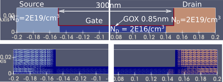 Fig. 1. (a) Structure and mesh of the simulated n-MOSFET with LG = 300nm. Similar p-MOSFET with p-source and drain is simulated. (b) Dopant
distribution in the simulated device with LG = 300nm.
Fig. 1. (a) Structure and mesh of the simulated n-MOSFET with LG = 300nm. Similar p-MOSFET with p-source and drain is simulated. (b) Dopant
distribution in the simulated device with LG = 300nm.
In this work, bulk electron and hole mobility in Silicon is set to 1450 cm2/Vs and 450 cm2/Vs, respectively. Channel mobility degradation is modeled using “Lombardi model”. Electron and hole lifetimes in the material are set to 1μsec.
Quantum confinement moves electron density away from the GOX/Silicon interface. This effect is modeled in the drift-diffusion simulations using three different models - Van Dort model, modified local density approximation (MLDA), and density gradient model.
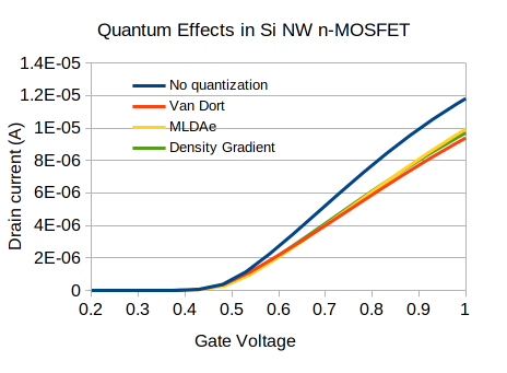
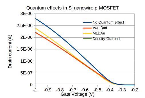
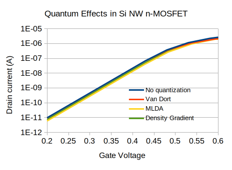
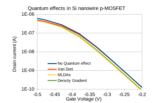
Comparison of the simulated transfer characteristics of the nanowire p- and n-MOSFETs with the measurements is shown in Fig. 2(a) and Fig. 2(b), for n- and p-MOSFETs of LG = 300nm, respectively. The figures show that on-state current is reduced when quantum confinement is taken into account. This is due to redistribution of carrier density due to quantum effects. In the on-state, electron (hole) density in nMOSFET (pMOSFET) shifts away from GOX/Si interface. This is shown in Fig. 4. Transfer characteristics are plotted on semilog-y scale in Fig. 3(a) and Fig. 3(b) to highlight the subthreshold region.
(a)
n-MOSFET |
(b)
p-MOSFET |
(a)
n-MOSFET |
(b)
p-MOSFET |
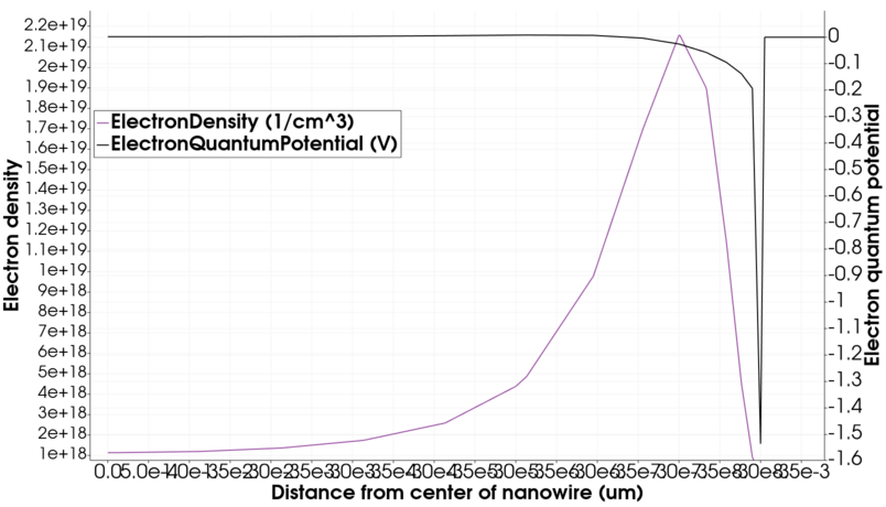 Fig. 4. Quantum potential and electron density are plotted perpendicular to GOX/Silicon interface at x=0. Right part after the peak is oxide, that before the
peak is Silicon. Quantum potential is highest at GOX/Si interface. Quantum potential is simulated using density gradient approach.
Fig. 4. Quantum potential and electron density are plotted perpendicular to GOX/Silicon interface at x=0. Right part after the peak is oxide, that before the
peak is Silicon. Quantum potential is highest at GOX/Si interface. Quantum potential is simulated using density gradient approach.
[1] Structure Generator and Mesher User Guide, SemiVi LLC, Switzerland, 2025.
[2] Drift-diffusion Solver User Guide, SemiVi LLC, Switzerland, 2025.
[3] C. Lombardi et al., “A Physically Based Mobility Model for Numerical Simulation of Non-planar Devices,” IEEE Trans. Computer-Aided Design, vol. 7, no. 11, pp. 1164-1171, 1988.