Schottky Diode Simulation With Periodic and Mirror Boundary Conditions
Saurabh Sant SemiVi LLC Zurich, Switzerland. saurabh.sant@semivi.ch
Abstract Schottky diode is simulated using SemiVi drift-diffusion solver under various boundary conditions (BCs) - mirror BC, Robin periodic BC, and mortar periodic BC. The study shows that mortar periodic BCs impose periodicity constraints exactly. Although Robin BCs do not impose exact periodic constraints, they are good enough for most of the applications. They are particularly good when mortar BCs create problems in convergence.
Index Terms Schottky diode, drift-diffusion, mortar periodic BC, Robin periodic BC, Mirror BC.
In forward biased Schottky diodes, current flow happens by a uni-polar transport - that is, either electrons or holes take part in conduction. Unipolar transport increases diode resistance at high currents, but it reduces forward voltage of the diode, making it suitable for low voltage applications. Also, faster switching can be achieved in Schottky diodes. Therefore, they are popular in high frequency applications.
In this work, we perform drift-diffusion simulations of a Schottky diode under three different boundary conditions (BCs) - mirror BC, Robin periodic BC, and mortar periodic BC. SemiVi structure generator and mesher is used to create the diode structure and to mesh it. Then, SemiVi drift-diffusion solver is used for simulating the diode with each of the the above mentioned BCs active, one at a time.
Simulation of drift-diffusion equations within a finite simulation domain activate zero flux BC at the domain boundary, by default. For Poisson equation, they are given by Eq. 1.
|
| (1) |
Similarly, for electron continuity equation, mirror BCs are given by Eq. 2.
 | (2) |
Also, for hole continuity equation, mirror BCs are given by Eq. 3.
 | (3) |
Here,  is unit normal at
  along the domain boundary (δΩ).
When the simulation domain is continuous at the boundary, the above BCs are equivalent to mirror BCs.
In ‘mortar’ periodic BC, vertices at the extrema along the axes of periodic BC are stitched together. In this case, the periodic BC is specified at Ymin. Therefore, vertices along the domain boundary at minimum of Y are stitched to those at the maximum of Y. Thus, for each of the equations, periodic BCs are given by,
 | (4) |
 | (5) |
 | (6) |
 | (7) |
In ‘robin’ periodic BC, vertices at the extrema along the axes of periodic BC are coupled together. Here, periodic BC is specified at Ymin. Therefore, vertices along the domain boundary at minimum of Y are coupled to those at the maximum of Y. Thus, periodic BCs for each of the equations are given by,
 | (8) |
 | (9) |
 | (10) |
 | (11) |
Here, α is an adjustable parameters set to 102.
We use SemiVi ‘Structure generator and Mesher’ to create the structure and a finite-element mesh for the device.
(a)
Device
Structure |
(b)
Periodic
Boundary
Conditions |
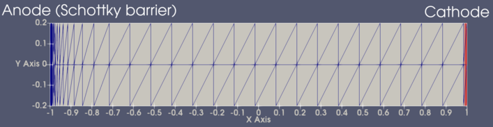
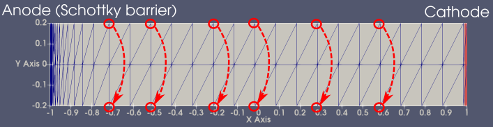
The pn-diode structure consists of a Silicon stripe of 400nm width and 2μm length. The Si stripe is uniformly doped with n-doping of 1017cm-3. A uniform mesh spacing of 100nm along y-direction. Along x-direction, mesh spacing increases gradually from 0.1nm at the Anode to 100nm at the cathode (see Fig. 1(a)). When periodic BC is imposed, the corresponding vertices on y-min and y-max boundary are paired as shown in Fig. 1(b). Note, that due to the symmetric structure of this device, mirror BC and periodic BCs should yield identical results.
Schottky barrier at the anode is set to 0.5eV. All the simulations are performed by quasistationary ramp to -2V and then another quasistationary ramp to 2V. SemiVi drift-diffusion simulator is used for all the device simulations.
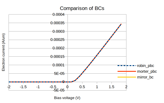
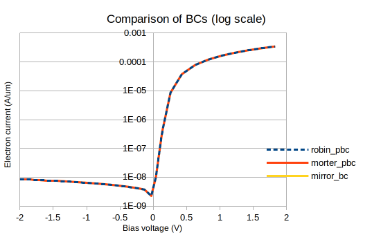
Current-voltage characteristics of the Schottky diode are shown in Fig. 2. On linear y-scale (see Fig. 2(a)), the diode characteristics look as expected with the diode forward voltage of 0.5V. Note, the linearity in the current at higher bias. This is a characteristic of a Schottky diode. Comparison of the IV characteristics using different BCs shows that electron current values are identical for all the three BCs, both on linear scale and on log scale (see Fig. 2(b)).
(a)
Electron
current
(linear
y-axis) |
(b)
Electron
current
(log
y-axis) |
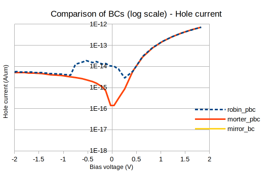
Since the device is a unipolar device with electrons as majority carriers, hole current is negligible compared to electron current. It is plotted on log scale in Fig. 3. Comparing the hole currents for all the three BCs shows that, hole currents match for mirror BC and mortar periodic BC. However, hole current is slightly different for robin BC. This is because, Robin BC imposes ‘less strict’ periodic condition compared to the mortar BC.
For exact periodicity, mortar BCs are preferred. However, in some case, mortar BCs may result in non-convergence. In that case, robin BCs can be used. Robin BCs, due to their ‘weaker’ nature, can yield better convergence, with little or no degradation of accuracy.
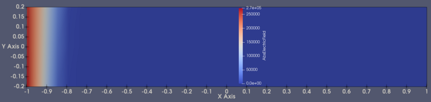
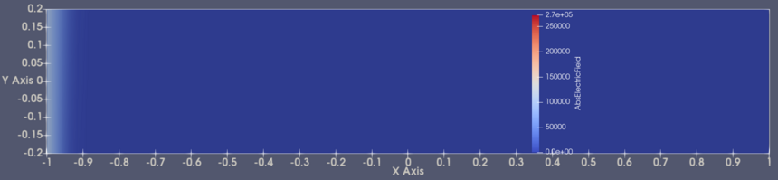
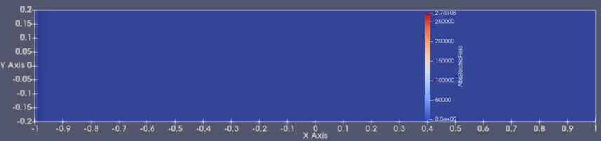
Spatial distribution of the magnitude of electric field | | throughout the device is given in Fig. 4. As expected, high electric field is
observed at the Schottky contact in the reverse bias, due to the presence of depletion region. At forward bias, small electric field is
present uniformly throughout the structure due to the electron current.
| throughout the device is given in Fig. 4. As expected, high electric field is
observed at the Schottky contact in the reverse bias, due to the presence of depletion region. At forward bias, small electric field is
present uniformly throughout the structure due to the electron current.
(a)
Reverse
bias of
2V |
(b) 0V
bias |
(c)
Forward
bias of
2V |
Similarly, spatial distribution of electron density throughout the device is given in Fig. 5. As expected, electrons are depleted at the Schottky contact in the reverse bias. At forward bias, electron density is uniform throughout the structure due to the electron injection.
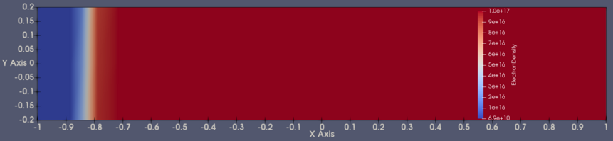
(a)
Reverse
bias of
2V |
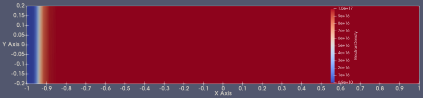
(b) 0V
bias |
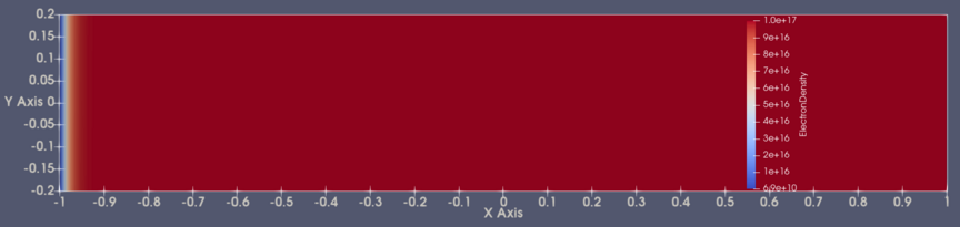
(c)
Forward
bias of
2V |
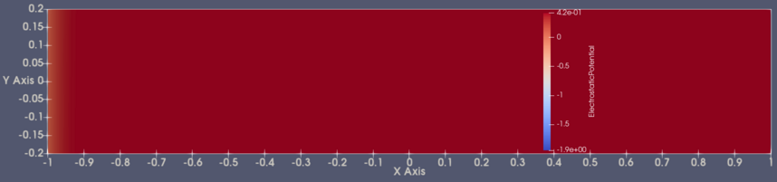
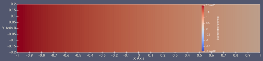
Spatial distribution of electrostatic potential throughout the device is given in Fig. 6. In reverse bias, electrostatic potential shows maximum variation at the Schottky contact. At forward bias, electrostatic potential has uniform ‘gradient’ throughout the device, due to the current flow.
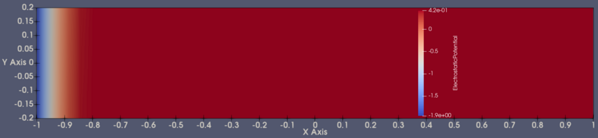
(a)
Reverse
bias of
2V |
(b) 0V
bias |
(c)
Forward
bias of
2V |