Mechanical stress induced mobility enhancement in
a double-gate MOSFET
Saurabh Sant
SemiVi LLC
Zurich, Switzerland.
saurabh.sant@semivi.ch
Abstract
Effect of mechanical stress along the channel and perpendicular to the channel on a double-gate n- and p-channel MOSFETs
is studied using SemiVi drift-diffusion solver. Mobility degradation due to interface roughness, doping, and high-field mobility
saturation is taken into account in the simulations. Transfer characteristics of the MOSFETs with stress along different directions
are compared to analyze the effect of stress.
Index Terms
Double-gate MOSFET, drift-diffusion, mechanical stress, FinFET.
I. Introduction
Performance improvement of the FinFETs can be achieved by improving channel mobility of electrons and holes in n- and p-channel
FinFETs, respectively. In modern FinFETs, mechanical stress is intentionally introduced on Silicon channel to improve e and h
mobility. Mechanical stress is typically process-induced during replacement gate process steps or induced by implanting Germanium in
source and drain of the FinFET.
In this work, we perform simulation study of n- and p-channel double-gate MOSFET (DG-MOSFET) in the presence of mechanical
stress. Also, different stress direction are used to analyze the effect of mechanical stress.
II. Mobility Degradation in Nano-scale MOSFET
As the source and the drain regions are heavily doped, resistance of a MOSFET often depends on the channel resistance. Presence of
impurities in the channel region increases scattering resulting in channel mobility degradation. In the SemiVi simulator, this is modeled
by activating Masetti model throughout the device.
Silicon/Gate-oxide interface often exhibits roughness, which adds to scattering of carriers in the inversion layer. This degrades
mobility of the carriers in the channel. This, surface-roughness induced mobility degradation is modeled by a model proposed by
Lombardi el al.
Carrier velocity is given by  = μ⋅
= μ⋅ , where
  is electric field.
  increases with
  . But this increase is sub-linear, and saturates at
high fields. This is due to the increased scattering at high electric field. This phenomenon is modeled by mobility saturation at “high
field”. We use a “High field saturation” model proposed by Canali el al.
. But this increase is sub-linear, and saturates at
high fields. This is due to the increased scattering at high electric field. This phenomenon is modeled by mobility saturation at “high
field”. We use a “High field saturation” model proposed by Canali el al.
The above models are implemented in ‘SemiVi’ drift-diffusion simulator and are activated throughout the device during the
simulations.
III. Mechanical Stress-induced Mobility Modulation
A. CB-edge shift
Silicon has six CB valleys which are degenerate (i.e. they have the same energy minimum). Applying compressive stress increases
energy of the valley-minima, while tensile stress decreases it. Applying anisotropic stress shifts different valleys by different energy, due
to symmetry reason. This energy shift per valley in the case of Silicon is given by.
 | (1) |
After calculating the CB edge shifts for all the valleys, CB edge is obtained as follows.
 | (2) |
B. VB-edge shift
VB maximum of Silicon is doubly degenerate, with two bands - LH and HH band - having the energy maxima at the Γ-point in the
reciprocal-lattice space. Similar to the CB, applying compressive stress increases energy of the valley-maxima, while tensile stress
decreases it. Due to the symmetry properties of the LH and HH bands, application of strain energetically separates LH and HH bands
and breaks degeneracy of the VB maxima. LH and HH energy shifts are derived from k.p theory without considering spin-orbit split-off
band. They are given by.
| ΔEV,hh = | a ⋅ (ϵxx + ϵyy + ϵzz) + δE | (3)
|
| ΔEV,lh = | a ⋅ (ϵxx + ϵyy + ϵzz) - δE | (4) |
 | (5) |
Here, a, b, and d are k.p parameters.
After calculating the VB edge shifts for all the bands, VB edge is obtained as follows.
 | (6) |
C. Mobility modification
Net e/h mobility is a weighted average of e/h mobility in each of the CB/VB valleys, weighted by the e/h occupancy of that
valley.
Application of strain breaks degeneracy of both CB and VB of Silicon. As a result, electron/hole re-population takes place. For
example, electrons populate all the six CB valleys equally in relaxed Si. In strained Silicon, more electrons occupy the CB valley(s)
with lower energy. As a result, net μe changes on application of strain. This is accounted in the drift-diffusion simulations by modifying
the mobility scaling factor (μr).
The above model is implemented in ‘SemiVi’ drift-diffusion simulator and is activated throughout the device during the
simulations.
IV. Simulation Setup
We use SemiVi ‘Structure generator and Mesher’ to create the DG-MOSFET structure and mesh it using the built-in
mesher.
A. Device Structure
The n-channel DG-MOSFET consists of a Silicon layer of thickness 20 nm and channel length of 100 nm. Source and drain of the
device have 50nm length. Silicon layer is doped with Boron doping of 2 × 10¹⁶/cm3, while source/drain are doped with Phosphorus
doping of 1019/cm3.
In the p-channel DG-MOSFET, the Silicon channel is doped with Phosphorus doping of 2 × 10¹⁶/cm3, while the source and the drain
are Boron doped with the doping of 1019/cm3.
Gate-oxide is composed of SiO2 with the thickness of 2nm on top and bottom of the stripe. Device structure and the doping
concentration is shown in Fig. 1(b).
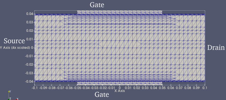
The device is meshed using ‘SemiVi’ mesher, which uses Quad-tree based ‘FEM meshing’. Since the channel region show sharp
changes in electron density, mesh near gate-oxide/Si interface is refined. Final mesh is shown in Fig. 1(a).
Transfer characteristics of the n-channel (p-channel) MOSFET are simulated by quasistationarily ramping the gate voltage from
0V to 1V (-1V) at a constant drain voltage of 1V (-1V). SemiVi drift-diffusion simulator is used for all the device
simulations.
V. Results and Discussion
A. Transfer characteristics
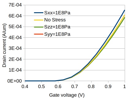
In n-channel DG-MOSFET simulation, a uniform tensile stress of 100MPa is introduced along x-axis (channel direction), y-axis, and
z-axis. Transfer characteristics of the DG-MOSFET simulated with stress along each of the three axes together with relaxed Silicon are
plotted in Fig. 2 at Vds = 1V. The plot shows, that tensile stress along the channel direction improves on-state current compared to the
relaxed Silicon. Whereas, tensile stress perpendicular to the channel degrades on-state current. This happens because tensile stress
breaks degeneracy the six CB valleys of Silicon. Tensile stress along x-axis lifts Δx-valley up compared to Δy,z valleys. As a
results, electrons re-populate Δy,z valleys. Due to anisotropy, Δy,z valleys offer low meff compared to Δx valley,
when the electron transport is along x-axis. As a result of low meff of Δy,z valleys together with re-population of
electrons into these valleys, overall mobility improves which increases on-state current. When stress is along either
of the y- or z-axes, Δx-valley is lowered. Owing to its high meff along x-axis, mobility degrades which decreases
on-current.
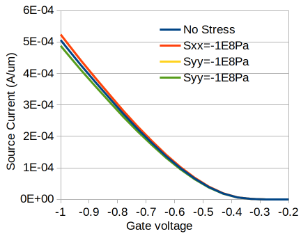
Similarly, in the simulations of p-channel DG-MOSFET, uniform compressive stress of 100MPa is applied along x-axis
(channel direction), y-axis, and z-axis. Transfer characteristics of the DG-MOSFET simulated with stress along each of
the three axes together with relaxed Silicon are plotted in Fig. 3 at Vds = -1V. The plot shows, that compressive
stress along the channel direction improves on-state current compared to the relaxed Silicon. This happens because
stress breaks degeneracy the two VB valleys of Silicon, namely HH and LH. Compressive stress along x-axis lifts
LH-valley up compared to HH valley. As a results, holes re-populate LH valley (note, higher the energy, more the
hole occupancy). LH-valley offers low meff compared to HH-valley. As a result of low meff of LH valley together
with re-population of holes into LH-valley, overall mobility improves which increases on-state current. When stress is
along either of the y- or z-axes, HH-valley is lifted up. Owing to its high meff, mobility degrades which decreases
on-current.