Effect of interface traps on a double-gate MOSFET
Saurabh Sant
SemiVi LLC
Zurich, Switzerland.
saurabh.sant@semivi.ch
Abstract
Effect of traps at gate-oxide/Silicon interface of double-gate n- and p-channel MOSFETs is studied using SemiVi drift-diffusion
solver. Mobility degradation due to interface roughness, doping, and high-field mobility saturation is taken into account in the
simulations. Transfer characteristics of the MOSFETs with different trap concentration are compared to analyze the effect of
interface traps.
Index Terms
Double-gate MOSFET, drift-diffusion, FinFET.
I. Introduction
Modern FinFETs use a thoroughly engineered gate-oxide stack of high-k dielectric together with SiO2. Although this gate-oxide
engineering achieves strong gate control of the channel, it results in defect formation at oxide/Silicon channel interface.
These defects (also called traps) can potentially shield channel from the gate, thereby weakening the gate control of the
channel.
In this work, we perform simulation study of n- and p-channel double-gate MOSFET (DG-MOSFET) to obtain transfer
characteristics with and without oxide/Silicon traps. Additionally, trap density at the interface is varied to study its effect on the transfer
characteristics.
II. Mobility Degradation in nano-scale MOSFET
As the source and the drain regions are heavily doped, resistance of a MOSFET often depends on the channel resistance. Presence of
impurities in the channel region increases scattering resulting in channel mobility degradation. In the SemiVi simulator, this is modeled
by activating Masetti model throughout the device.
Silicon/Gate-oxide interface often exhibits roughness, which adds to scattering of carriers in the inversion layer. This degrades
mobility of the carriers in the channel. This, surface-roughness induced mobility degradation is modeled by a model proposed by
Lombardi el al.
Carrier velocity is given by  = μ⋅
= μ⋅ , where
  is electric field.
  increases with
  . But this increase is sub-linear, and saturates at
high fields. This is due to the increased scattering at high electric field. This phenomenon is modeled by mobility saturation at “high
field”. We use a “High field saturation” model proposed by Canali el al.
. But this increase is sub-linear, and saturates at
high fields. This is due to the increased scattering at high electric field. This phenomenon is modeled by mobility saturation at “high
field”. We use a “High field saturation” model proposed by Canali el al.
The above models are implemented in ‘SemiVi’ drift-diffusion simulator and are activated throughout the device during the
simulations.
III. Modeling trapping and de-trapping
During device operation, various trapping/de-trapping of electrons and holes take place simultaneously. Rates of these processes
determine occupancy of the traps.
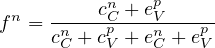
Occupancy of the trap levels depends on the rates of charging and discharging of the traps. Electron occupation factor fn of the trap
level is determined by net rate of capture of CB electrons rCn minus net rate of capture of VB holes rV p. This is given by,
 | = rCn - r
V p | (1a)
|
| rCn | = (1 - fn) ⋅ c
Cn - fn ⋅ e
Cn | (1b)
|
| rV p | = (1 - fp) ⋅ c
V p - fp ⋅ e
V p | (1c)
|
| fp | = 1 - fn | (1d) |
In steady-state electron occupancy at a trap level fn as follows.
 | (2) |
A. Capture and emission rates
Capture and emission rates used in the above equation depend on various factors including trap energy level, carrier
density, and the current density. Capture rate of an electron from the CB and that of a hole from the VB is given by,
| cCn | = σ
n | (3a)
|
| cV p | = σ
p | (3b) |
Here, σn∕p are electron/hole capture cross-sections, vthn and vthp are thermal velocities of electron and hole. The model parameters
gn∕pJ determine proportionate contribution of n and of | n| to the total capture rate.
| eCn | = σ
n ⋅ vthn ⋅ n1∕g
n | (4a)
|
| eV p | = σ
p ⋅ vthp ⋅ p1∕g
p | (4b)
|
| n1 | = NC exp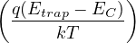 | (4c)
|
| p1 | = NV exp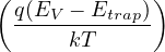 | (4d) |
where, gn∕p are degeneracy factors, Etrap is the trap energy level, and NC∕V are CB and VB DOS.
When traps are used in the device, the above (de-)trapping processes are simulated in ‘SemiVi’ drift-diffusion simulator to calculate
trap occupancy and the rates. When occupied, “donor” traps are neural, else they are positively charged. Similarly, when occupied,
“acceptor” traps are negatively charged, else they are neutral. This charge state of the traps is taken into account in Poisson
equation.
IV. Simulation Setup
We use SemiVi ‘Structure generator and Mesher’ [?] to create the DG-MOSFET structure and mesh it using the built-in
mesher.
A. Device Structure
The n-channel DG-MOSFET consists of a Silicon layer of thickness 20 nm and channel length of 100 nm. Source and drain of the
device have 50nm length. Silicon layer is doped with Boron doping of 2 × 10¹⁶/cm3, while source/drain are doped with Phosphorus
doping of 1019/cm3.
In the p-channel DG-MOSFET, the Silicon channel is doped with Phosphorus doping of 2 × 10¹⁶/cm3, while the source and the drain
are Boron doped with the doping of 1019/cm3.
Gate-oxide is composed of SiO2 with the thickness of 2nm on top and bottom of the stripe. Device structure and the doping
concentration is shown in Fig. 1(b).
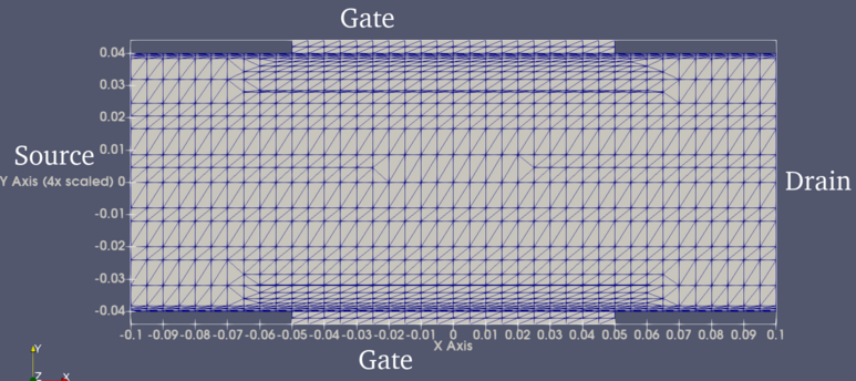
The device is meshed using ‘SemiVi’ mesher, which uses Quad-tree based ‘FEM meshing’. Since the channel region show sharp
changes in electron density, mesh near gate-oxide/Si interface is refined. Final mesh is shown in Fig. 1(a).
Transfer characteristics of the n-channel (p-channel) MOSFET are simulated by quasistationarily ramping the gate voltage from 0V
to 1V (-1V) at a constant drain voltage of 1V (-1V). SemiVi drift-diffusion simulator [?] is used for all the device
simulations.
V. Results and Discussion
A. Transfer characteristics
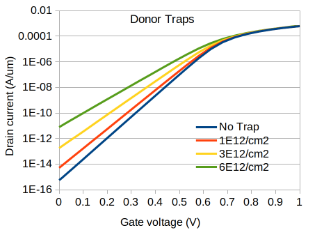
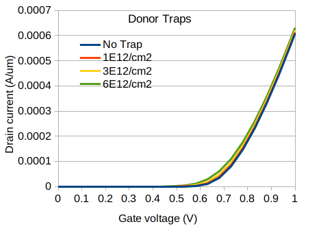
In the simulation of n-channel DG-MOSFET, donor type oxide/Silicon interface traps are simulated. The trap density (Dit) is varied
from 0 to 6 × 10¹²∕cm2 in the simulations. Transfer characteristics of the DG-MOSFET are plotted in Fig. 2(a) at Vds = 1V. The plot
shows, that as Dit increases, transfer characteristics become less steep in the subthreshold region. That is, subthreshold swing of the
MOSFET increases. Transfer characteristics plotted in Fig. 2(b) confirm that on-state current is somewhat affected by increase of
Dit.
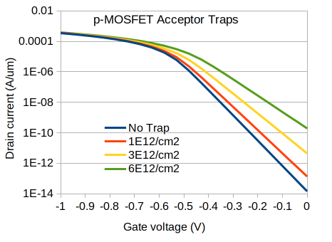
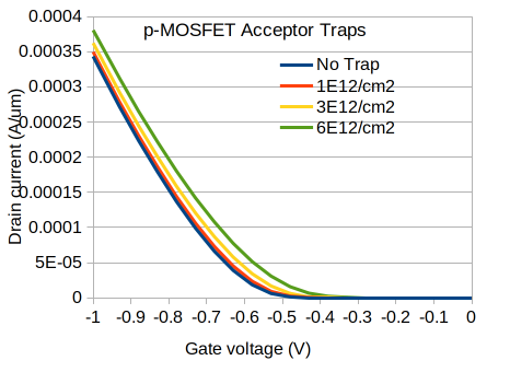
Similarly, in the simulations of p-channel DG-MOSFET, acceptor-type oxide/Silicon interface traps are simulated.
The trap density is varied from 0 to 6 × 10¹²∕cm2 in the simulations. Transfer characteristics of the DG-MOSFET
are plotted in Fig. 3(b) at Vds = -1V. The plot shows, that as Dit increases, subthreshold swing of the MOSFET
increases. Transfer characteristics plotted in Fig. 3(a) confirm that on-state current is somewhat affected by the increase of
Dit.
Reason for the increase of the subthreshold swing is, that increase of Vgs increases trap occupancy, thereby shielding the channel
region from the gate voltage. This decreases gate coupling of the channel, and subthreshold swing increases.