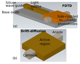
 Fig. 1. (a) Structure of a photodiode coupled to the Silicon waveguide used for the optical simulations, (b) Photodiode connected by p- and n- stripes at
the opposite sides of the square.
Fig. 1. (a) Structure of a photodiode coupled to the Silicon waveguide used for the optical simulations, (b) Photodiode connected by p- and n- stripes at
the opposite sides of the square.
Optical and Electrical Simulation of In0.53GaAs Photodiode for Internal Quantum Efficiency Calculation
Saurabh Sant SemiVi LLC Zurich, Switzerland. saurabh.sant@semivi.ch
Abstract In this work, light propagation in a rectangular photodiode coupled to a waveguide is studied using finite-difference- time-domain (FDTD) simulations. Additionally, drift-diffusion simulations of the photo-diode are performed to calculate internal quantum efficiency of the photo-diode. For that purpose, spatial distribution of optical field obtained by the FDTD simulations is imported to the drift-diffusion simulator to accurately model spatial variation of optical generation of electron-hole pairs in the photodiode structure.
Index Terms Opto-electronics, photo-diode, drift-diffusion, In0.53GaAs .
Ultra-fast and broad-band detectors of optical signal are de- sired for fiber-optic communications. Monolithically integrated photo diodes are particularly useful as receiver. For accurate prediction of the efficiency of the photodiodes, they must be simulated in both optical and electrical domains.
In this work, a traditional rectangular photo-diode is simulated in optical domain by finite-difference-time-domain (FDTD) simulations and in electrical domain by drift-diffusion simulations. Internal quantum efficiency (IQE) is calculated using the simulation results.
Fig. 1. (a) Structure of a photodiode coupled to the Silicon waveguide used for the optical simulations, (b) Photodiode connected by p- and n- stripes at
the opposite sides of the square.
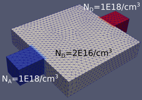
The structure used for simulation in the optical domain consists of In0.53GaAs photo-diode, Silicon waveguide, and the oxide layer from the SOI wafer. It is shown in Fig. 1(a). The waveguide has a 260nm x 260nm cross-section and a length of 3µm. The photodiode consists of a square of side length of 1.3µm and thickness of 260nm. The p/n stripes of length 350nm connect the photodiode to the electrical contacts. Drift-diffusion simulations are performed on the photo-diode and p/n-stripe structure shown in Fig. 1(b).
The photodiode is intrinsically doped with n-doping of 2 × 10¹⁶/cm3. Doping of the p/n-stripes are set to 1018/cm3. Both the optical simulation structure of Fig. 1(a) as well as drift- diffusion simulation structure of Fig. 1(b) are generated and meshed using SemiVi structure generator and mesher [2].
The optical structure is simulated using SemiVi hardware- accelerated FDTD simulator [4]. Details on the optical simulation of the
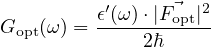
photodiode are provided in [1]. Optical generation in a semiconductor is proportional to the local | |2. Optical electric field is
obtained from the FDTD simulations and imported to SemiVi drift-diffusion simulator. Internally, it is interpolated to the vertices of the
unstructured mesh of the electrical simulation structure. Rate of electron-hole pairs due to the illumination is given
by,
|2. Optical electric field is
obtained from the FDTD simulations and imported to SemiVi drift-diffusion simulator. Internally, it is interpolated to the vertices of the
unstructured mesh of the electrical simulation structure. Rate of electron-hole pairs due to the illumination is given
by,
 | (1) |
Here, ϵ′(ω) is the imaginary part of the dielectric permittivity of In0.53GaAs for the given light wavelength, and ℏ is reduced Planck’s constant. Importing optical field to simulate optical generation captures non-uniformity of optical generation.
Electron and hole mobilities in the drift-diffusion simulation are set to 300 cm2/Vsec and 100 cm2/Vsec, respectively. They are taken from the mobility measurement in TASE- grown In0.53GaAs -on-insulator for MOSFET application. Electron and hole life-times are set to 10-9 sec, following the calibration [3].
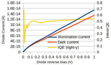
In the drift-diffusion simulations, the photo-diode is quasistationarily ramped to the reverse bias of 1V. Simultaneously, optical generation is also ramped to is value corresponding to the light intensity of 70mW/m2. ‘Illumination current’, thus obtained, is plotted together with the ‘dark current’ (without optical generation) in Fig. 3. Internal quantum efficiency (IQE) which is a fraction of optically generated e-h pairs collected at the anode/cathode is calculated from the two currents as follows.
 | (2) |
This IQE is also plotted in Fig. 3 vs diode bias.
Spatial distribution of optical generation and net recombination (SRH recombination minus optical generation) is plotted in Fig. 4 at the reverse bias of -1V. Integrating optical generation reveals that the photodiode structure collects 22000 photons/sec.
In this way, we have used SemiVi FDTD solver together with SemiVi drift-diffusion solver for opto-electronic simulations to calculate internal quantum efficiency (IQE) of the monolithically integrated In0.53GaAs photodiode.
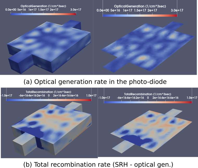 Fig. 4. In the photo-diode, spatial distribution of (a) optical generation, (b) net recombination (SRH recombination - optical generation) in side-contact
diode
Fig. 4. In the photo-diode, spatial distribution of (a) optical generation, (b) net recombination (SRH recombination - optical generation) in side-contact
diode
[1] S. Sant,“Study of Hexagonal Photo-Diode for Efficient Side-Coupling to Silicon Wave-Guide,” 2025 International Conference on Numerical Simulation of Optoelectronic Devices (NUSOD), Lodz, Poland, 2025, pp. 105-106.
[2] Structure Generator And Mesher User Guide, SemiVi LLC, Switzerland, 2025.
[3] S. Sant et al,“Impact of Floating Body Effect, Back-Gate Traps, and Trap-Assisted Tunneling on Scaled In0.53Ga0.47As Ultrathin-Body MOSFETs and Mitigation Measures,” in IEEE Transactions on Electron Devices, vol. 65, no. 6, pp. 2578-2584, June 2018.
[4] FDTD Solver User Guide, SemiVi LLC, Switzerland, 2025.
[5] Drift-diffusion Solver User Guide, SemiVi LLC, Switzerland, 2025.