 | (1a) |
 | (1b) |
 | (1c) |
 | (1d) |
Hardware-accelerated Opto-Solver for FDTD and BPM Simulations
Abstract We have developed hardware-accelerated Finite-Difference Time-Domain (FDTD) solver and Beam-Propagation-Method (BPM) solver which use Graphic Cards for parallel computation. These solvers are nearly 4 to 8 times faster than the multi-threaded solvers which use multi-threaded CPU. We employ these solvers to compute wave propagation through the Silicon waveguide coupler. Both FDTD and BPM simulations show that a fraction of mode in the active waveguide enters the adjacent waveguide in the coupled section. Also, We compare computation speed using the GPU accelerated and multi-threaded versions of the solvers with two precision - 32-bit and 64-bit previsions. GPU acceleration yields a speed-up of 8.5 and 1.82, respectively, in FDTD and BPM simulations.
Index Terms Hardware-acceleration, FDTD solver, BPM solver, Silicon waveguide, coupler.
Ever-increasing usage of AI brings forth the necessity of large data-centers. Servers in these data-centers use ultra-fast optical cables for data-transfer. Each of these servers stand to benefit from Silicon photonic modules which can be used for off-chip communications between processors, as well as for data-transceivers. These Si photonic modules are designed and optimized by performing optical simulations using Finite-Difference Time-Domain (FDTD) method [1] and Beam-Propagation-Method (BPM) [2]. These methods are known to be computationally demanding, but are also parallelizable, thereby, reducing computation time. The smaller the simulation time, the faster the iterative optimization procedure would be.
Modern hardware such as Graphics Processing Units (GPU) tend to have a large number of processing cores (called shaders). Running a computationally demanding but parallelizable application on the GPU can deliver performance gains compared to its run on a multi-threaded CPU. However, developing a software which utilizes GPU computation is a complex task and requires in-depth knowledge of Cuda libraries, in case of Nvidia GPUs.
To assist the optical simulation experts with faster runs, we, at SemiVi, have developed hardware-accelerated FDTD solver application [3] which runs on a CPU as well as on a GPU. Together with that, we have also developed hardware-accelerated BPM solver [4] for calculation of steady-state optical response of the photonic Structures. We employ both FDTD and BPM solvers to study a Silicon waveguide coupler structure.
Maxwell’s equation describe the response of a material system in the absence of electric charges to an electromagnetic excitation (with ρ = 0).
Here,  = ϵ
= ϵ is a displacement vector, E is an electric field,
  =
=  ∕μ is the magnetic flux, and
  is the magnetic
field.
is the magnetic
field.
Out of Maxwell’s equations, Eq. 1a and Eq.1b are always satisfied by FDTD algorithm. Eq. 1c links spatial variation of electric field
vector ( ) with temporal variation of magnetic flux vector (
 ) and Eq. 1d links spatial variation of
  with temporal variation of
  .
The LHS of Eq. 1c can be expanded and its x,y,z components can be equated to those of the RHS which gives,
.
The LHS of Eq. 1c can be expanded and its x,y,z components can be equated to those of the RHS which gives,
Above set of equations form  update equations. Similarly, the LHS of Eq. 1d can be expanded to get update equation for electric
field. In FDTD algorithm, these two equations (Eq. 1c and Eq. 1d) are alternately solved on a special rectangular (cubic, in 3D) grid
called Yee grid at every half-time step. That is, Eq. 1c is solved at time-step i while Eq. 1d is solved at time-step i +
update equations. Similarly, the LHS of Eq. 1d can be expanded to get update equation for electric
field. In FDTD algorithm, these two equations (Eq. 1c and Eq. 1d) are alternately solved on a special rectangular (cubic, in 3D) grid
called Yee grid at every half-time step. That is, Eq. 1c is solved at time-step i while Eq. 1d is solved at time-step i +  [5].
[5].
In all the simulations, we use convolutional perfectly matched layer (CPML) boundary condition along all the six faces of the
cuboidal boundary surface. A CPML introduces a special region in the first n = 10 layers nearest to the boundary. During an  update
in this special region, an additional displacements coming from convolutional functions is added to it to cancel out the reflections
coming from the finite domain boundary at the surface.
update
in this special region, an additional displacements coming from convolutional functions is added to it to cancel out the reflections
coming from the finite domain boundary at the surface.
In BPM implementation, mode is set to propagate in x- direction. Splitting ∇ operator and  into transverse and longitudinal
components, we get,
into transverse and longitudinal
components, we get,
![[ ]
∂2E⃗t- 2 ⃗ ∂tn2- ⃗ 2 2⃗
∂x2 + ∇tEt + ∇t n2 ⋅Et + n k0Et = 0](GPU_FDTD_BPM_Solvers20x.png) | (3) |
. In a waveguide, rapid variation of the transverse fields is the phase variation due to propagation along the propagation axis. One can
define a Spatially Varying Envelope(SVE) of the transverse  t as follows,
 | (4) |
The above equation can be used to calculate  . Substituting SVE of
  t, and expressions for
  and
and  in Eq. 3, we get
Eq. 5 form the equations used for propagating the mode along x direction in a BPM solver [6].
We use the ‘Structure generator and Mesher’ [7] to create the structure and a regular cubic mesh for FDTD and BPM simulations.
(a)
Layout
of the
coupler |
(b)
Coupler
structure
generated
from
layout |
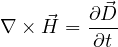
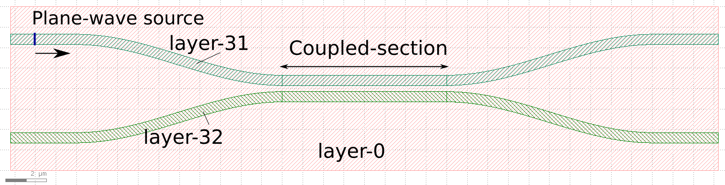
The structure consists of two Silicon waveguides which propagate along x-direction. They are coupled in the middle 8μm region. Layout of these waveguides is shown in Fig. 1(a). The structure generator takes the GDS layout file as an input and creates the waveguide structure. The structure consists of Oxide base of thickness 480nm created from ‘layer-0’ and two Si waveguides of thickness 240nm created using ‘layer-31’ and ‘layer-32’. Vacuum padding of 240nm is used along y- and z-direction, while that of 1.1μm is used along x-direction. The simulated structure is shown in Fig. 1(b).
Mesh spacing of 50nm, 20nm, and 50nm are used along x-, y- and z-directions. This spacing creates a 3D grid of 765 × 61 × 251 grid-points. There are 11,712,915 vertices in this cubic grid.
The Si waveguide of ‘layer-31’ is excited by a uniform plane-wave source at 200nm away from the left boundary. The source of intensity 1000W and wavelength of 1.35μm, is placed in the plane perpendicular to the waveguide and is confined to the cross-section of the waveguide.
Convolutional perfectly matched layer (CPML) boundary conditions (BCs) are active at all the boundaries of the simulation domain. The CPML BCs are active on the last five boundary layers parallel to ‘XZ’ and ‘XY’ planes, and on last ten boundary layers parallel to ‘YZ’ plane. All the boundary layers are located in the ‘vacuum’ padding.
Perfectly Matched Layer (PML) BC is active at the boundaries parallel to ‘XY’ and ‘XZ’ planes on the nearest five boundary layers. The PML ensures that light incident on the boundary is absorbed in these layers.
FDTD simulations are performed on the coupler structure for 500 fsec which corresponds to 8900 time-steps. At time 490 fsec, electric and magnetic fields are post-processed to calculate intensity. Spatial distribution of intensity is plotted in Fig. 2. As seen in the figure, a fraction of light from the active waveguide is transmitted to the adjacent waveguide in the coupling region. Coupling strength can be increased further by bringing the waveguide structures closer to each other.
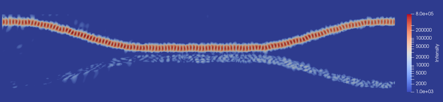 Fig. 2. In FDTD simulations, spatial distribution of intensity in the horizontal cross-section at the middle of the waveguide height (i.e. 120nm above the
base-oxide). The figures show that, a tiny fraction of optical power is transferred from the illuminated waveguide to the adjacent one. Note, that a color-map
with log scale is used.
Fig. 2. In FDTD simulations, spatial distribution of intensity in the horizontal cross-section at the middle of the waveguide height (i.e. 120nm above the
base-oxide). The figures show that, a tiny fraction of optical power is transferred from the illuminated waveguide to the adjacent one. Note, that a color-map
with log scale is used.
Absolute electric field at each vertex is averaged from time 450 fsec to 490 fsec. It is plotted in Fig. 3 on linear scale. Notice that weak coupling between the active and the adjacent waveguide causes a small field to be present in the adjacent waveguide.
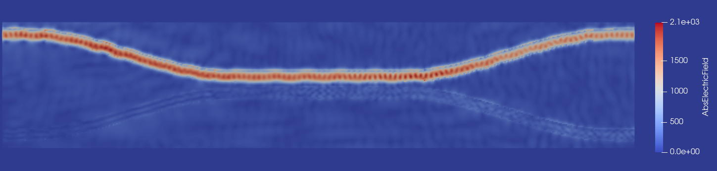 Fig. 3. In FDTD simulations, spatial distribution of abs. electric field in the horizontal cross-section at the middle of the waveguide height (i.e. 120nm above
the base-oxide). The figure shows that, a small fraction of the waveguide signal enters the adjacent waveguide in the middle region.
Fig. 3. In FDTD simulations, spatial distribution of abs. electric field in the horizontal cross-section at the middle of the waveguide height (i.e. 120nm above
the base-oxide). The figure shows that, a small fraction of the waveguide signal enters the adjacent waveguide in the middle region.
Envelope functions Ψy and Ψz are calculated by the BPM solver starting from the source and propagating the fields along positive
x-direction. These functions correspond to the amplitude of the electric fields along the waveguide in the ‘steady-state’. Absolute
electric field ( ) is calculated as post-processing step. Spatial distribution of absolute electric field is plotted in Fig. 4.
The figure shows that a small fraction of light entering in the adjacent waveguide, similar to what is observed in FDTD simulations.
) is calculated as post-processing step. Spatial distribution of absolute electric field is plotted in Fig. 4.
The figure shows that a small fraction of light entering in the adjacent waveguide, similar to what is observed in FDTD simulations.
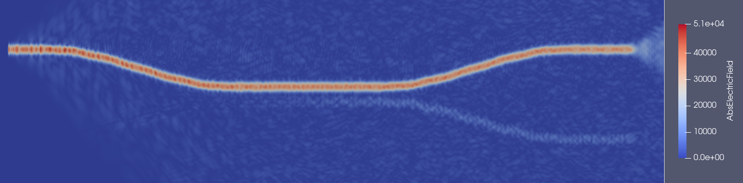 Fig. 4. In BPM simulations, spatial distribution of abs. electric field in the horizontal cross-section at the middle of the waveguide height (i.e. 120nm above
the base-oxide). The figure confirms the findings of FDTD simulations.
Fig. 4. In BPM simulations, spatial distribution of abs. electric field in the horizontal cross-section at the middle of the waveguide height (i.e. 120nm above
the base-oxide). The figure confirms the findings of FDTD simulations.
C. Speed-up By Hardware-acceleration
Hardware-accelerated FDTD solver and BPM solver are used to speed up the calculations, particularly for large structures such as the coupler structure shown above. Nvidia ‘RTX-3090’ GPU is used as a hardware for the above simulations. To understand usefulness of the GPU, the simulations are also performed using a 4-threaded CPU ‘i3-2100’ without using the GPU. For both the GPU and CPU simulations, the solver software is compiled using two floating point precision, namely, 32-bit and 64-bit float. Computation times for the above FDTD simulation on the GPU and the CPU for the two precision are compared in Table I. The table shows that, for both 32-bit and 64-bit precision, the GPU delivers faster performance compared to the 4-threaded CPU. As expected, 32-bit computation takes less time compared to 64-bit computation. Also, the GPU delivers nearly 8.5 times speedup for FDTD simulations compared to the CPU. It is observed, that higher speedup is observed for longer FDTD simulations i.e. the simulations which use more time-steps.
| Hardware | 64-bit FDTD | 32-bit FDTD |
| CPU | 1hr 56m 40s | 1hr 30m 5s |
| RTX-3090 | 20m 50s | 10m 40s |
| Speed-up | 5.60 | 8.45 |
Comparison of BPM simulation time using the GPU and the CPU is presented in Table II. The table confirms that using the GPU delivers faster simulation, but the observed speed-up is not as high as in the case of FDTD solver. The reason seems to be as follows. In the BPM solver, the GPU is used only for the sparse matrix system solving step, since it is the most time-consuming step. All the other computations are performed on the CPU. Perhaps, moving all the other computations (apart from matrix solving) to the GPU will deliver better speed-up.
| Hardware | 64-bit BPM | 32-bit BPM |
| CPU | 2m 2s | 2m 26s |
| RTX-3090 | 1m 33s | 1m 20s |
| Speed-up | 1.33 | 1.82 |
We have presented hardware-accelerated finite-difference time-domain (FDTD) and beam-propagation-method (BPM) solvers for optical simulations. We perform FDTD and BPM simulations of Silicon waveguide coupler structure using these solvers. When only one of the waveguide carries optical signal, the other waveguide receives a fraction of the signal owing to the proximity of the two waveguides in the middle section of the coupler. Both, FDTD and BPM simulations confirm this effect. Additionally, we compare simulation times of FDTD and BPM simulations by using hardware-accelerator - GPU - and by using multi-threaded CPU. In the case of FDTD simulations, use of the GPU achieves speed-up of up to 8.5 times. On the other hand, speed-up of iPod 1.82 times is achieved when the GPU is used for the BPM simulations.
[1] J. Young, ”Photonic crystal-based optical interconnect,” in IEEE Potentials, vol. 26, no. 3, pp. 36-41, May-June 2007.
[2] S. Makino, T. Fujisawa and K. Saitoh, ”Wavefront Matching Method Based on Full-Vector Finite-Element Beam Propagation Method for Polarization Control Devices,” in Journal of Lightwave Technology, vol. 35, no. 14, pp. 2840-2845, 15 July15, 2017.
[3] FDTD Solver User Guide, SemiVi LLC, Switzerland, 2025.
[4] BPM Solver User Guide, SemiVi LLC, Switzerland, 2025.
[5] J. Schneider, “Understanding the Finite-Difference Time-Domain Method,” www.eecs.wsu.edu/~schneidj/ufdtd, 2010.
[6] G. Pedrola , “Beam Propagation Method for Design of Optical Waveguide Devices,” October 2015, ISBN: 978-1-119-08340-5.
[7] Structure Generator and Mesher User Guide, SemiVi LLC, Switzerland, 2025.


![[ 1 ∂(n2) 1 ∂ (n2) ]
n2-∂y--Ψy + n2--∂z-Ψz](GPU_FDTD_BPM_Solvers31x.png)


![[ ]
1-∂(n2) 1-∂(n2)
n2 ∂y Ψy + n2 ∂z Ψz](GPU_FDTD_BPM_Solvers36x.png)