 Fig. 1. Hexagonal In0.53GaAs photo-diode at the end of Si waveguide, with two configurations (a) and (b). (c) rectangular photo-diode coupled to the
waveguide at the end. (d) Waveguide embedded in oxide cladding.
Fig. 1. Hexagonal In0.53GaAs photo-diode at the end of Si waveguide, with two configurations (a) and (b). (c) rectangular photo-diode coupled to the
waveguide at the end. (d) Waveguide embedded in oxide cladding.
Study of Hexagonal Photo-diode for Efficient Side-coupling to Silicon Wave-guide
Saurabh Sant SemiVi LLC Zurich, Switzerland. saurabh.sant@semivi.ch
Abstract We present the study of a hexagonal photo-diode design for efficient top/side coupling to Silicon waveguide optimized for 1.35μm wavelength. We calculate the coupling strength between the waveguide and the photo-diode by using hardware-accelerated finite-difference time-domain (FDTD) simulations. In the study, hexagonal geometry of the photo-diode is compared with the conventional rectangular stripe-based diode. The study shows, that use of hexagonal geometry enables better coupling between the wave-guide and the photo-diode. This is achieved by the activation of the whispering-gallery-like internal reflections happening inside the hexagonal photo-diode.
Index Terms Silicon photonics, photodiode, hexagonal whispering gallery mode, hardware-accelerated FDTD solver.
Recent advancements in AI have brought the necessity of large data-centers to the forefront. High-speed optical data-receivers in these data-centers requires ultra-fast and broad-band detection of optical signals. Monolithically integrated photodiodes (PD) are well suited for the receiver applications [1]. Performance and speed of the PDs can be improved by shrinking the structure. Structure shrinkage while still ensuring sufficient coupling strength can be achieved by using plasmonic enhancements [2] or by utilizing a hexagonal geometry which exhibit whispering-gallery modes (WGM). The Template Assisted Selective Epitaxy (TASE) technology [3] enables monolithic integration of III-V materials on a Si platform and allows for side-coupling of Si waveguide with InGaAs PD. In this study, we design a side-coupled waveguide photodetector in hexagonal geometry and compare its strength with that of the conventional rectangular photodetector. For the structure design and simulation, we use the hardware-accelerated FDTD simulator by SemiVi [4].
In order to study the effect of hexagonal structure on coupling strength of the photodiode, we performed a comparative study of two photo-diode geometries - traditional rectangular stripe, and hexagonal whispering-gallery-like structure. The two structures are shown in Fig. 1. Note that, the waveguide and the diode are embedded in the cladding oxide as shown in Fig. 1(d). The cladding oxide is hidden in the other figures. The simulation domain is defined by a cubic box of ‘vacuum’ around the structure such that there is padding of 0.32μm on all sides of the cuboid.
Fig. 1. Hexagonal In0.53GaAs photo-diode at the end of Si waveguide, with two configurations (a) and (b). (c) rectangular photo-diode coupled to the
waveguide at the end. (d) Waveguide embedded in oxide cladding.
The waveguide cross-section is optimized for compactness and mode-confinement. The optimized waveguide cross-section of 260nm × 260nm is used for this study. This waveguide has a TM mode with the refractive index of 2.37. The mode confinement is shown in Fig. 2(b). Length of the waveguide is 2.15μm. Hexagonal In0.53GaAs photo-diode structure has a side-length of 0.65μm, which is set such that the diode can exhibit a whispering-gallery-like mode at the refractive index of 2.44. Modes of the hexagonal structure are shown in Fig. 2(d) and (e). The rectangular structure has a side-length of 1.3μm. In all the structures, the waveguide and the photo-diode are separated by a 200nm oxide layer. Cubic grid-spacing of 20nm is used along x,y,z axes in all the FDTD simulations.
 Fig. 2. (a) Cross-section of the waveguide and (b) Modal field in it. (c) Lateral cross-section of the hexagonal InGaAs disc. (d) and (e) Whispering gallery
modes supperted by it.
Fig. 2. (a) Cross-section of the waveguide and (b) Modal field in it. (c) Lateral cross-section of the hexagonal InGaAs disc. (d) and (e) Whispering gallery
modes supperted by it.
B. Light source and boundary conditions
Coupling strength of waveguide and photo-diode structures is probed by exciting the waveguide by a uniform plane-wave source at 200nm away from the end. The source of intensity 1000W and wavelength of 1.35μm, was placed in the plane perpendicular to the waveguide and was confined to the cross-section of the waveguide.
Convolutional perfectly matched layer (CPML) boundary conditions (BCs) were active at all the boundaries of the simulation domain. The CPML BCs were active on the last ten boundary layers. All the boundary layers were located in the ‘vacuum’ padding.
The above structures and mesh are created by the Python interface of the ‘Structure Generator and Mesher’ by SemiVi. It is simulated using the hardware-accelerated FDTD simulator by SemiVi [4]. Nvidia GPU ‘GTX3090’ is used for FDTD simulations.
FDTD simulations were performed for 200 fsec (8994 time-steps). At time of 190 fsec, spatial intensity is calculated in the photo-diode. In a photo-diode, electron-hole generation is proportional to the light intensity at that location. Current generated by the photo-diode is proportional to the integrated spatial intensity. Integration of the intensity is performed and presented in Table I. The table shows that, integrated intensity in the photo-diode region of the side-coupled and top-coupled hexagonal structures is higher than that in the traditional rectangular structures. This confirms, that hexagonal whispering-gallery-like structure provides better coupling to the waveguide. It is likely to provide better sensitivity.
Fig. 3 shows absolute spatial distribution of electric field averaged over the last 20 fsec in the horizontal cut-plane in the three designs. The figure shows that the field develops a peculiar pattern in the hexagonal structures similar to the WGMs. The hexagon in Fig. 3(a) exhibits superposition of WGM with the waveguide, whereas that in Fig. 3(b) primarily shows the WGM. In contrast, rectangular PD in Fig. 3(c) does not exhibit these modes and shows lower coupling with the waveguide.
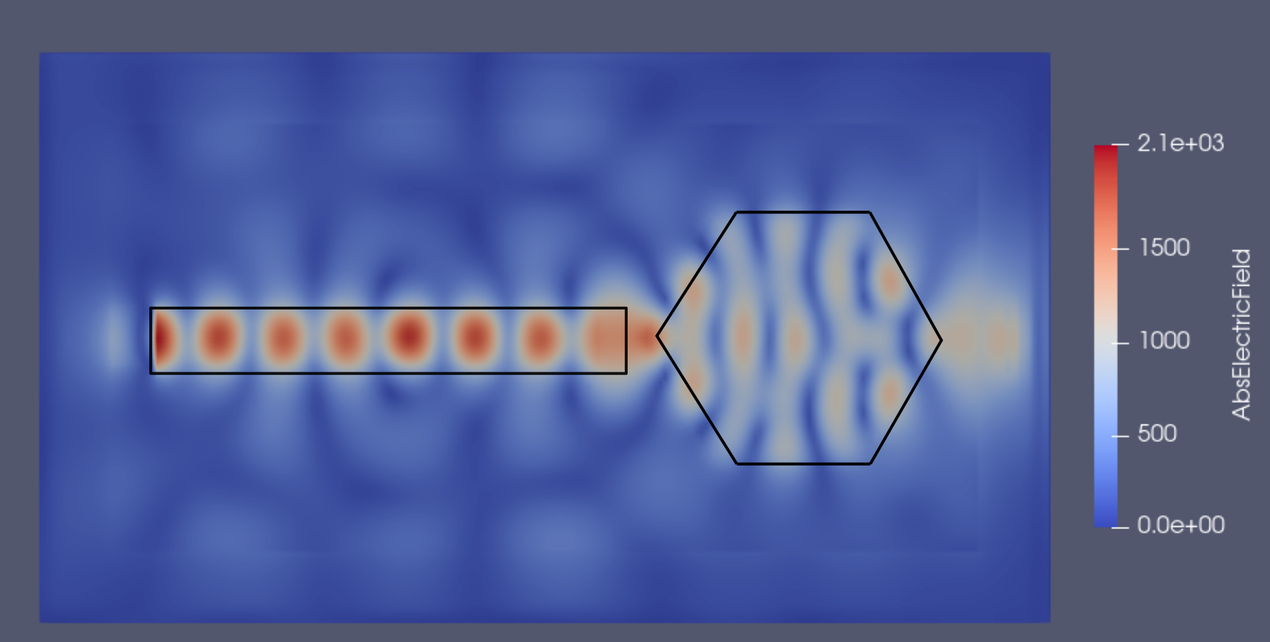
(a)
Hexagonal
Photodiode |

(b)
Rotated
Hexagonal
Photodiode |
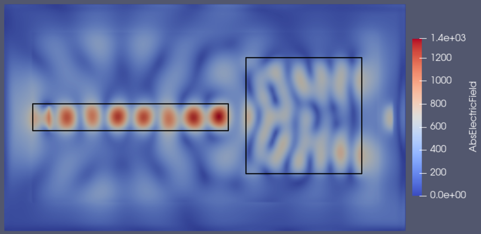
(c)
Rectangular
Photodiode |
| Structure | Integrated abs. field | Integrated intensity |
| V/m*μm3 | W/m2*μm3 | |
| WGM diode type-I | 245.5 | 413.18 |
| WGM diode type-II | 221.77 | 378.87 |
| Rect. diode | 167.49 | 206.99 |
We studied the effect of hexagonal whispering-gallery-like photodiode structure on the coupling strength between Silicon wave-guide and In0.53GaAs photodiode. Geometry of the waveguide and the hexagonal photodiode are designed such that the hexagonal structure exhibits whispering-gallery mode close to the refractive index of the waveguide. The system is simulated by using the FDTD solver by SemiVi and the coupling strength between the waveguide and the photodiode. Simulations confirm that hexagonal structures increase the waveguide-photodiode coupling, compared to the traditional rectangular structure. This is due to the whispering-gallery modes of the photodiode.
[1] P. Wen Eli al, “Waveguide coupled III-V photodiodes monolithically integrated on Si,” Nature Communications 13, 909, 2022.
[2] J. Gosciniak and M. Rasras, “High-bandwidth and high-responsivity waveguide-integrated plasmonic germanium photodetector,”J. Opt. Soc. Am. B 36, 2481, 2019.
[3] H. Schmid et al “Template-assisted selective epitaxy of III–V nanoscale devices for co-planar heterogeneous integration with Si,” Applied Physics Letters 106(23), 233101, 2015.